Photo-Electric Capacitor Memory based on Ge-Nanocrystals
Project Director: Dr. Toma STOICA
Project ID: 89PED from 03/01/2017 (PN-III-P2-2.1-PED-2016-0286)-PhotoElCaNanoMem
Project Director: Dr. Toma Stoica
Project Type: National
Project Program: PED
Funded by: Romanian National Authority for Scientific Research, UEFISCDI
Contractor: National Institute of Materials Physics
Project Status: In progress
Start Date: Tuesday, 3 January, 2017
End Date: Monday, 2 July, 2018
Project Abstract:
The main goal of the project is the fabrication of photoelectric Ge nanocrystals based memories for eco-nanotechnology applications, combining an optical sensor with a nonvolatile electronic memory in a single new device. In such device, both the electric field and the light can control the charge injection into the Ge nanocrystals (NCs) and thus the memory states of the device. It may work as a photoelectric sensor floating gate memory, or a photoelectro switch floating gate memory for event detection reversible device, with applications to security systems, intelligent home systems, integrated silicon photonics, etc. The used materials and fabrication technology are ecofriendly and compatible with silicon technology. In this project, the demonstrator is designed as a transparent electrode oxide semiconductor (MOS type) capacitor memory with Ge NCs in oxide matrix, NCs being coupled to the Si substrate through a thin tunnel oxide. The active layers will be fabricated by magnetron sputtering deposition followed by rapid thermal annealing. The charge exchange between the substrate and the Ge NCs can be controlled by electric field applied between the substrate and a gate (top) contact. At intermediary voltages, the capacitance-voltage characteristic shows hysteresis. The charge retention can be optimized for long term or dynamic memory. For top illuminated demonstrator proposed by this project, a transparent electrode will be used and the retention dynamic will be optimized for photoelectric control of charge storage. The device operation is based on the generation of electrons and holes pairs under illumination and by this activation of the tunneling process resulting in changes of the hysteresis states. The novelty of the proposed project consists in realization of a photosensitive GeNCs floating gate memory, tuning the structure of the demonstrator in order to obtain simultaneously electrical and optical control of the memory effect.
Project Objectives:
The main goal of the project is the fabrication of photoelectric Ge nanocrystals based memories for eco-nanotechnology applications, combining an optical sensor with a nonvolatile electronic memory in a single new device. In such device, both the electric field and the light can control the charge injection into the Ge nanocrystals and thus the memory states of the device.
Dr. Toma Stoica
Dr. Constantin Logofatu
Dr. Valentin Adrian Maraloiu
Dr. Ana Maria Lepadatu
Dr. Adrian Slav
Dr. Catalin Palade
Technician Elena Stan
First stage (2017): Fabricarea si caracterizarea structurilor de memorie foto-electrice pe baza de Ge-NCs in matrice oxidica.
Layer structures based on Ge nanocrystals (NCs) were fabricated using magnetron sputtering deposition on c-Si substrates for obtaining floating gate photo-electric memories that can be programed by both electric field and light. The structure consists in: thin tunneling HfO2; floating gate of Ge-HfO2; and control oxide of HfO2. After deposition Ge nanocrystals are obtained by rapid thermal annealing at 600oC.
The layer structures have been investigated using HRTEM (High resolution transmission electron microscopy) and HAADF-STEM (high angle annular dark field-scanning TEM) imaging in order to obtain information about film composition, size, location and crystallinity degree of the Ge nanoparticles. The crystallinity was also investigated using Raman scattering spectroscopy and the fit of the Ge-Ge Raman peak is in agreement with TEM results on Ge nanocrystals size. The composition and the position of Ge nanocrystals at the expected position of floating gate layer was confirmed by XPS (X-ray Photoelectron Spectroscopy) measurements.
The contacts of the memory capacitors were obtained by vacuum evaporation of semitransparent Au on top and Al to the bottom of the p-Si substrate. The electrical characterization regarding the resistivity and dielectric constant of the component layers was obtained by simulation of the frequency dispersion curve of the capacitance in the regime of carrier accumulation. [1]
The effect of the light exposure during the programming of the capacitor memory based on Ge nanocrystals in HfO2 was investigated. The light influence on the C-V curves after erasing at negative voltage is negligible, but can produce changes of capacitance ratio Q up to 60% for C-V data measured after 10 min writing at positive voltage under light illumination (5 mW/cm2). The reduction of the writing time to 1 min increases the capacitance changes Q to 90%. [2]
References
- Material parameters from frequency dispersion simulation of floating gate memory with Ge nanocrystals in HfO2, C. Palade, A.M. Lepadatu, A. Slav, S. Lazanu, V.S. Teodorescu, T. Stoica, M.L. Ciurea, Applied Surface Science 428 (2018) 698–702.
- Light illumination effects on floating gate memory with Ge nanocrystals in HfO2, C. Palade, A. Slav, A.M. Lepadatu, S. Lazanu, M.L. Ciurea, T. Stoica, IEEE International Semiconductor Conference - CAS Proceedings (2017), pp. 87–90
Final stage (2018): Fabrication and functional testing of PEGNM demonstrator - TRL3
In this stage, optoelectric floating gate memory devices based on Ge NCs in HfO2 were obtained. Functional testing was performed in laboratory using different operation procedures. The operation modes are defined as a function of detection modes of the effects induced by light: M1 – corresponding to the effect of the light pulses on the capacitance at different gate voltages (M1a), or on the flat band voltage during the retention time measurements (M1b); M2 – corresponding to the effect of a continuous illumination on hysteresis curve, including the writing periods at cycle ends; M3 – corresponding to the effect of the writing at cycle ends by electric field+light on hysteresis curve, the hysteresis being measured in the dark. Three types of optoelectric memory structures S1 – S3 with various thicknesses of the tunnel and control oxides have been obtained and tested. The selected PEGNM fabrication procedure was described in details, including the following technological steps and fabrication parameters: chemical cleaning of the Si substrates followed by magnetron sputtering deposition of the three layer structure of Ge and HfO2; rapid thermal annealing for Ge NCs formation as a floating gate; deposition of transparent electrodes either semitransparent Au or transparent conductive oxides (TCO) by magnetron sputtering deposition; deposition by vacuum evaporation of back side Al electrodes; and finally the bonding of the sample with a matrix of 4 individual memories on an alumina chip carrier. Schematic of the cross-section of the optoelectric floating gate memory and the bonded matrix of 4 elements are shown by the figure below. The structure S3 was selected as optimal for the actual stage of the device as TRL3 demonstrate, and based on this structure and the operation mode M1b, a patent application was submitted at OSIM Romania.
The fabrication and testing of the electrooptic memories base on Ge NCs offered us the possibility to analyze and model the tunnelling charge transfer phenomena that take place between Ge NCs and Si substrate through the tunnel HfO2 layer, as well as setting the functional operation parameters for PEGNM demonstrator. In this way, the different operation modes of optoelectric memory structures have been quantitatively characterized. Thus, sensibilities of the photoeffects on the flat band up to 130 mV/mJ for a device area of 1 mm2 were demonstrated. Also, electrons injection up to 1.6 electrons into a single NC was detected for integral illumination of 20mW/cm2. Spectral dependence of the hysteresis window increase by illumination shown a maximum contribution of the light of wavelenght of about 950 nm, corresponding to photo-effect in both Ge NCs and Si substrate. Scientific results will be published within ISI journals and presented at international conferences.
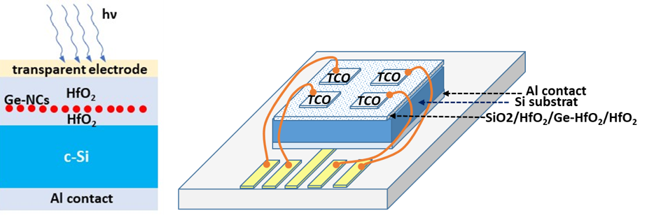
Schematic cross-section of optoelectric memory structure and a matrix of four memories on a chip carrier.
List of Publications:
- Material parameters from frequency dispersion simulation of floating gate memory with Ge nanocrystals in HfO2, C. Palade, A.M. Lepadatu, A. Slav, S. Lazanu, V.S. Teodorescu, T. Stoica, M.L. Ciurea, Applied Surface Science 428 (2018) 698–702.
- Light illumination effects on floating gate memory with Ge nanocrystals in HfO2, C. Palade, A. Slav, A.M. Lepadatu, S. Lazanu, M.L. Ciurea, T. Stoica, work awarded at CAS 2017 conference, published in EEE International Semiconductor Conference - CAS Proceedings (2017), pp. 87–90.
International conference presentations:
- Ge nanocrystals in oxides with memory and photoelectrical properties, C. Palade, A. Slav, A.-M. Lepadatu, A.V. Maraloiu, S. Lazanu, C. Logofatu, T. Stoica, V.S. Teodorescu, M.L. Ciurea, The 9th International Conference on Advanced Materials - ROCAM 2017, July 11-14, Bucuresti.
- Ge nanocrystals as charge storage nodes in floating gate capacitor memories with HfO2, A.-M. Lepadatu, C. Palade, A. Slav, A.V. Maraloiu, S. Lazanu, C. Logofatu, T. Stoica, V.S. Teodorescu, M.L. Ciurea, 17-th Int. Balkan Workshop on Applied Physics, Constanta, 11-14 iulie 2017.
- Active materials based on Ge NCs in oxides for trilayer memory capacitors and photosensitive structures, A. Slav, C. Palade, A.-M. Lepadatu, A.V. Maraloiu, C. Logofatu, S. Lazanu, T. Stoica, V.S. Teodorescu, M.L. Ciurea 17-th Int. Balkan Workshop on Applied Physics, Constanta, 11-14 iulie 2017.
- Light illumination effects on floating gate memory with Ge nanocrystals in HfO2, C. Palade, A. Slav, A.M. Lepadatu, S. Lazanu, M.L. Ciurea, T. Stoica, work awarded at International Semiconductor Conference - CAS Proceedings (2017).
Project Contact Person:
Project Director: Dr.Toma Stoica
National Institute of Materials Physics, Atomistilor 405A., 077125 Magurele - Bucharest, ROMANIA
Tel:+40--(0)21-2418-171
Email: toma.stoica@infim .ro
PROJECTS/ NATIONAL PROJECTS
Copyright © 2024 National Institute of Materials Physics. All Rights Reserved