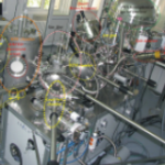
Experimental Cluster for Surface and Interface Science
FACILITIES / STIINTA-SUPRAFETEI

The Cluster represents one of the most complex such systems in Europe, makes possible the preparation and characterization in situ of surfaces and interfaces, and consists of three
mutually coupled units :
- The MBE (Molecular Beam Epitaxy) Chamber;
- The STM (Scanning Tunneling Microscope) Chamber;
- The Spin- and Angle-resolved Photoelectron Spectroscopy (SARPES).
All chambers operate in ultrahigh vacuum (UHV), the base pressure ranges from 1-2 x 10⁻¹⁰mbar to 10-11 mbar range The overall value of the whole system exceeds 1.3 M€. The employed techniques are:
In the MBE chamber:
- preparation facilities:
- sample heating up to 1200 °C; cooling down to 77 K;
- evaporation from a 4-target e-beam evaporator;
- evaporation from a high temperature Knudsen cell (2000 °C);
- controlled gas adsorption and desorption;
- monitor of thicknesses using a quartz microbalance.
- in situ characterization:
- LEED (Low Energy Electron Diffraction);
- RHEED (Reflection High Energy Electron Spectroscopy);
- AES (Auger Electron Spectroscopy);
- Quadrupole Mass Spectroscopy (thermal induced desorption, photodesorption);
In the STM chamber:
- sample preparation stage (heating, ion sputtering);
- tip preparation (ion sputtering);
- variable temperature (77 – 453 K) scanning tunneling microscopy (STM);
- scanning tunneling spectroscopy (STS);
In the SARPES chamber:
- conventional X-ray photoelectron spectroscopy using a dual (Al/Mg Kα) anode;
- high resolution XPS using a monochromatized dual (Al Kα /Ag Lα) source;
- ultraviolet photoelectron spectroscopy (UPS);
- angle-resolved XPS: x-ray photoelectron diffraction (XPD);
- angle-resolved UPS (ARUPS): band structure, Fermi surface, etc.;
- spin-resolved UPS: spin-polarized density of states;
- angle- and spin-resolved UPS: spin-polarized band structure;
- programable ion sputtering: depth profiling;
- flood gun for sample neutralization;
- electron gun for AES; medium energy ion scattering spectroscopy (MEIS).The performance of the complex system described above is illustrated in Fig. 2 for high resolution photoelectron spectroscopy and in Fig. 3 for scanning tunneling microscopy with atomic resolution.
The performance of the complex system described above is illustrated in Fig. 2 for high resolution photoelectron spectroscopy and in Fig. 3 for scanning tunneling microscopy with atomic resolution.
Copyright © 2024 National Institute of Materials Physics. All Rights Reserved