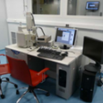
Scanning Electron Microscope S-3400 N (Hitachi) with Quantum Elphy Nanolithography System and Laser Interferometer Ultra Precision Positioning Strage (Raith)
FACILITIES / NANOFABRICATION-OF-MATERIALS

The nanolithography facility of SEM is esential for preparation of nanostructures and for contact definition with a resolution of about 100 nm. A nanolithography equipment comprises besides the standard SEM feature, a facility with computer controlled electron beam for direct “writing” the small size features directly onto the sample surface. A special CAD software is employed for writing the desired features for defining the nanostructures or electrical contact. A exposure sensitive polymer can be employed to defining of the exposed and nonexposed areas. The procedure can be used for preparing samples with nanodots, nanowires, nanotubes, nanorods of semiconductor or oxidic materials. Actual preparation of nanostructures and/or contacts is completed by chemical etching in the cleanroom or by etching in a focused ion beam equipment.
Equipment components :
- Hitachi S3400 SEM
- Raith ELPHY Quantum Electron Beam Lithography
- Raith High Precision Positioning Stage with Laser Interferometer
- Deben PCD Beam Blanker
- Probe current meter Keithley 6845 Picoammeter
- Beamblanker Driver Electronics
- Dedicated Software
Technical specifications :
- High Vacuum and Low Vacuum
- Computer controlled 5 axis Motorised stage
- 5 segment High Response, High Sensitivity Backscattered Detector
- SE detector for High Vacuum
- The ability to reproducibly achieve feature size below 50 nm by EBL
- Multilayer EBL with less than 20 nm overlay
Copyright © 2024 National Institute of Materials Physics. All Rights Reserved