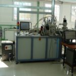
Deposition of semiconductor thin films and multilayer structures by magnetron sputtering: dielectrics (SiO2, TiO2, ZrO2, HfO2, Al2O3, Si3N4) and semiconductors (Si, Ge, SiGe, SiGeSn) on heated substrates or on substrates mantained at room temperature Configuration in situanalysis techniques: Auger electron surface spectroscopy – AES low-energy electron diffraction – LEED real time in situellipsometric monitoring and profilometer for […]
View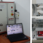
Rapid thermal annealing (RTA) and controlled oxidations (RTO) in the rapid thermal processing – RTP system (up to 3-inch silicon wafer) at 200 – 1250 °C with ramp rates up to 200 °C/s, in gas flow (N2, O2, Ar si H2) and thermal annealing in the three independent temperature zone horizontal split tube furnace at temperatures up to 1200 °C […]
View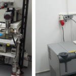
Electrical characterization in dark and under illumination and Hall investigations by measurements and modelling of experimental curves: current-voltage (I– V) at different temperatures T, in DC and AC regime capacitance-voltage (C– V), capacitance-frequency (C – f) and capacitance-time (C – t) polarization-voltage (P– V) I– T and R – T at different bias voltages Photocurrent spectra (I– λ) under modulated and continuous light regime Hall measurements: V–Icharacteristics for different applied currents, […]
View