National Institute Of Materials Physics - Romania
Atomic Structures and Defects in Advanced Materials (LASDAM)
Facilities and Services
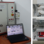
Rapid thermal annealing (RTA) and controlled oxidations (RTO) in the rapid thermal processing – RTP system (up to 3-inch silicon wafer) at 200 – 1250 °C with ramp rates up to 200 °C/s, in gas flow (N2, O2, Ar si H2) and thermal annealing in the three independent temperature zone horizontal split tube furnace at temperatures up to 1200 °C […]
View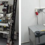
Electrical characterization in dark and under illumination and Hall investigations by measurements and modelling of experimental curves: current-voltage (I– V) at different temperatures T, in DC and AC regime capacitance-voltage (C– V), capacitance-frequency (C – f) and capacitance-time (C – t) polarization-voltage (P– V) I– T and R – T at different bias voltages Photocurrent spectra (I– λ) under modulated and continuous light regime Hall measurements: V–Icharacteristics for different applied currents, […]
View
Machines: Wire saw Lapping machines Zeiss Axio Observer reversed metallographic microscope for monitoring the thinning/polishing stages Zeiss Stemi 2000 stereoscopic optical microscope for TEM specimen manipulation Gatan PIPS ion milling installations JEOL JEE 4C vacuum evaporator Gatan ultrasound disc cutter Gatan Dimple Grinder
View
CW X-band EPR spectrometer model EMXplus from Bruker (upgraded Varian E12) Operating parameters: Frequency range: 9.2 – 9.9 GHz; Sensitivity: 1010 spins/Gauss; Magnetic field: 0.03 – 1.8 T; Temperature: 90 – 300 K.
View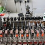
Specifications Carrier gas : synthetic air (5.0 purity) with controllable relative humidity (RH: 0–90%) and flow (10–200 ml/min); Test gases: CO, CH4, NO2, H2S, NH3, SO2 Description Flow system is used to dose different target gas concentrations under dynamic regime. It consists of eleven individual channels (dry synthetic air, humid synthetic air, NO2, CO, CH4, […]
View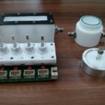
Description Within the sensors chambers up to four gas sensors with different electrodes configurations can be simultaneously exposed to the gas atmosphere. Subsequent Teflon sockets and stainless steel electrical contacts are used for DC measurements and sensor’s temperature control. The two parts of the chamber, the main body and the cover are sealed using Viton […]
View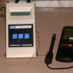
Precise gas flow control is crucial for acquiring accurately gas concentrations. Therefore mass flow controllers must be periodically calibrated using Alltech DFC. Calibrated Testo 625 thermo hygrometer is used to check the relative humidity accuracy through the flow system.
View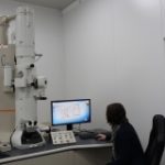
A multifunctional tool designed for the research and characterization of advanced materials, used for the following types of studies: conventional transmission electron microscopy, high-resolution transmission electron microscopy, electron tomography, in-situ electron microscopy at high or low (cryogenic) temperature, energy dispersive X-ray spectroscopy, elemental chemical mapping. TECHNICAL SPECIFICATIONS Scanning Transmission Electron Microscopy (STEM) unit with Annular […]
ViewCopyright © 2026 National Institute of Materials Physics. All Rights Reserved