National Institute Of Materials Physics - Romania
Functional Nanostructures
Facilities and Services
Equipment Circular Dichroism Spectrometer J-815, JASCO Spectroradiometer CS 2000, Konica Minolta Surftest SJ-210- Series 178-Portable Surface Roughness Tester, Mitutoyo FR-pOrtable, ThetaMetrisis Slot-Die Coater, Ossila: https://www.ossila.com/products/slot-die-coater Four-Point Probe: https://www.ossila.com/products/four-point-probe-system Contact Angle Goniometer: https://www.ossila.com/products/contact-angle-goniometer Thin film deposition installation UCL2878 Impedance Spectrometer w. PeakTech DC power supply 6075 Services OLED or similar devices characterization
View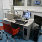
The nanolithography facility of SEM is esential for preparation of nanostructures and for contact definition with a resolution of about 100 nm. A nanolithography equipment comprises besides the standard SEM feature, a facility with computer controlled electron beam for direct “writing” the small size features directly onto the sample surface. A special CAD software is […]
View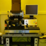
The equipment for optical litography allows for selectively masking and exposing of certain areas of the sample surface, using a “mask” or a set of masks. Masks are realized in advance by laser etching a thin metalic layer deposited onto a special glass slide. Masking is necessary for the operations of selective etching or “lift-off”. […]
View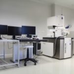
Equipment for high resolution electron printing that will be used to realize various types of structures and electrical contacts on nano-objects supergrid periodic applications in photonics and other metallization with complex geometries required for the development of advanced materials structures, for different applications. TECHNICAL SPECIFICATIONS High resolution electron lithography equipment will combine high-resolution scanning electron […]
View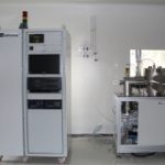
The equipment is intended for necessary research needed to obtain new heterostructures with applications in microelectronics, optoelectronics, renewable energy, advanced sensors and for applications in medicine, energy storage. TECHNICAL SPECIFICATIONS Substrate size: 2 inches; Base vacuum chamber in deposit: 10-5 mbar; Substrate temperature: 550 oC; Gas Lines: 2, with flow control; Automatic and computerized control […]
View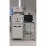
The equipment will be used for the deposition of carbon-based materials, such as graphene, nanotubes, possibly SiC, necessary for developing heterostructures of interest, including such materials. TECHNICAL SPECIFICATIONS Substrate size: 2 inches; Base vacuum chamber in deposit: minimum 10-5 mbar; Substrate temperature of 1400 oC; Gas Lines: 5, with flow control; Automatic and computerized control of […]
View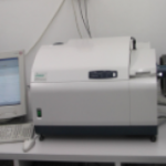
The Jasco MCD spectrometer allows the measurement of both optical transmission and photoluminescence for the UV-vis spectral domain. The measurements can be performed in a magnetic field of 1.4 T and to temperatures down to liquid nitrogen by means of a cryostat.
View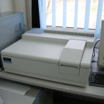
Technical details : excitation sources: tungsten and deuterium lamps double monochromator equipped with 1140tr/mm (UV/VIS range) and 360 tr/mm (NIR range) gratings detectors: R6872 (UV/VIS range) and PbS-Peltier effect cooled (NIR range) photomultipliers beam splitter: 46 Hz chopper Acquisition & control software: UV WinLab 5.2.0 accessories: integrating sphere and universal reflectance accessory Performances : spectral […]
View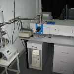
Technical details : excitation source: 450 W Xe lamp monochromators (excitation emission): f/3.6 Czeny-Turner, double grating, all reflective optics diffraction gratings: classically ruled, 1200 tr/mm; blaze 330nm (MEx) and 500nm (MEm) emission signal detector: at room tempe-rature-R928P side-on photomultiplier tube (180-850nm); software package: FluorEssence 2.0 (powered by Origin 7.5) Performances : excitation range: 240-600nm […]
View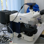
Technical details: reflexion, transmission and fluorescence microscopy filter cubes for different UV and visible wavelength
ViewCopyright © 2026 National Institute of Materials Physics. All Rights Reserved