National Institute Of Materials Physics - Romania
Optical Processes in Nanostructured Materials
Facilities and Services
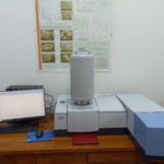
Technical details:-excitation source: YAG:Nd laser ( 1064 nm) 500mW, horizontally polarized (H)-Michaelson interferometer: ROCKSOLID configuration, permanently aligned-alignment excitation source: HeNe laser, 633 nm, 1mW-Excitation radiation rejection: NOCH filter-Detector: Ge-diode, cooled at liquid nitrogen temperature (77K)-Acquisition &Control software: OPUS 8.5Performances:-spectral domain: 50-3600 cm-1 (Stokes shift), -resolution: 1 cm-1Experiment types:FT-Raman180o (back scattering) and 90o (right angle) measuring geometriesFT-Raman Microscope180o (back scattering) […]
View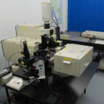
Technical details:– the T64000 Raman system is composed of a pre-monochromator and a spectrograph stage; – the pre-monochromator, working as a tunable filter is a double subtractive monochromator equipped with two 1800 gr/mm diffraction gratings.– the spectrograph stage, used as disperser is provided with a two grating-turret (one of the two gratings of 1800gr/mm and the other […]
View
Technical details:-KBr beamsplitter & RT-DLaTGS detector (mid-infrared)-T222/3 multilayer beamsplitter & RT-DTGS-FIR detector– Michaelson interferometer: ROCKSOLID configuration, permanently aligned;-alignment excitation source: HeNe laser, 633 nm, 1mW-Acquisition & control software: OPUS 6.0– accessories: ATR devicePerformances:-standard spectral range: 370-7500 cm-1-far IR extension: 50-680 cm-1-resolution: 2 cm-1 Services offered to users: analysis by IR spectroscopy in the geometry of […]
View
Technical details:– Michaelson interferometer; 57 mm dynamically aligned, 60° air bearing Michelson – KBr beamsplitter; – Optical microscope for infrared range Cary 610: Collection objective: 15x IR/Visible all-reflecting on-axis Schwarzchild objective; NA = 0.62, working distance = 21 mm; Includes slide-on Ge micro ATR (Provides 1.1 um pixel size) – detector: Wideband MCT 100 μm […]
View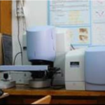
Characterization of the material, located in microscopic regions, of a solid, liquid, powder or paste sample, by means of the characteristic absorption in the IR. Fast scanning allows studying the kinetics of chemical reactions or a dynamic process of obtaining (forming) a material. Characterisation: FTIR spectroscopy on FTIR imaging microscope. 7800-600 cm-1, Image Pixel 6.25μ; […]
View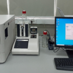
Technical details: – radiation source: introduction of radiation from a 780 nm LED in an integrative sphere ensures an intense and homogeneous radiation in space; – measuring places: flow cell with two channels, illuminated area 4.5 mm2; – detection: with extreme sensitivity sensor, two strings of diodes 1024 pixels; – resolution of the refractive angle: […]
View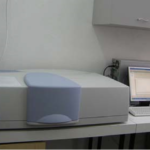
Technical details:-excitation sources: tungsten and deuterium lamps-double monochromator equipped with 1140 tr/mm (UV/VIS range) and 360 tr/mm (NIR range) gratings-detectors: R6872 (UV/VIS range) and PbS-Peltier effect cooled (NIR range) photomultipliers-beam splitter: 46 Hz chopper-Acquisition & control software: UV WinLab 5.2.0-accessories: integrating sphere and universal reflectance accessoryPerformances:-spectral range: 175-3300 nm-resolution: δ 0.05nm (UV/VIS), δ 0.2 nm (NIR)-wavelength precision: […]
View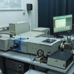
Technical details:-excitation source: 450 W Xe lamp-monochromators (excitation emission): f/3.6 Czeny-Turner, double grating, all reflectiveoptics-diffraction gratings: classically ruled, 1200 tr/mm; blaze 330 nm (MEx) and 500 nm(MEm)-emission signal detector: at room tempe-rature-R928P side-on photomultiplier tube(180-850nm);-software package: FluorEssence 2.0 (powered by Origin 7.5) Performances:-excitation range: 240-600 nm-emission range: 290-850 nm-photomultiplier response linearity: 2×10⁶ cps (in photon […]
View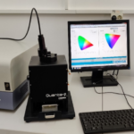
Quantum yield and colorimetric characterization of solid (powders) and liquid phosphors Technical details:– Jobin Yvon FluoroMax-4P with integration sphere assembly, luminescence detection range 350-800nm, -For powders or liquids samples – Dedicated software for quantum yield and colorimetry characaterizationPerformances:– absolute quantum efficiency and colorimetric parameters (CIE 1931) Services offered to users: colorimetric analysis (CIE diagram) and quantum efficiency […]
View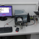
Optical imaging and spectroscopical characterization of various luminescent objects with different sizes down to the microns range. Technical details:– laser beam 454nm excitation sourceT222/3 multilayer beamsplitter & RT-DTGS-FIR detector– luminescence detection range 400-800nm with cooled CCD camera – Transmission modePerformances:– optical resolution down to 1micron Services offered to users: Luminescence imaging and optical spectroscopy characterization […]
ViewCopyright © 2026 National Institute of Materials Physics. All Rights Reserved