National Institute of Materials Physics
In the present project we aim at developing field effect transistors with multisegment nanowire channels and studying their charge and spin transport properties. The channel material will be either CdTe or pure and doped ZnO. The structures will be obtained using a combination of electrochemical deposition in ion track membranes for fabricating multisegment metal –semiconductor – metal nanowires, nanowire manipulation, lithographical techniques and focused ion beam induced metallization (FIB –IM).
We aim at replacing the classical approach for preparing transistors with nanowire channels moving from uniform nanowires to nanowires with the composition modulated along the nanostructure length. We proved the concept of multisegment nanowires in our previous research regarding nanowire diodes, the present project representing a natural step forward. Thus, in Figure 2 several images of different uniform and multisegment wires prepared by the project leader’s group are presented. Such complex nanostructures will constitute the building blocks of the field effect transistors.
Milestone 1 (M.1.): Controlled placement of multisegment nanowires on Si/SiO2 substrates.
(A.1.1): Preparation of multisegment nanowires by template replication.
(A.1.2.) Morphological, compositional and structural characterization of multisegment nanowires
(A.1.3.) Placement of nanowires on substrates
Milestone 2 (M.2.): Fabrication of a field effect nanowire based device with CdTe channel
(A.2.1): Preparation of a multisegment nanowire with drain and source segments defined by overpotential modulation based on CdTe.
(A.2.2.): Preparation of interdigitated electrodes on Si/SiO2 substrates by lithographical techniques
(A.2.3.): Placement of CdTe multisegment nanowires on electrode systems and contacting.
(A.2.4.): Complex characterization of nanowires and nanowire devices
Milestone 3 (M.3.): Fabrication of a field effect nanowire based device with ZnO channel
(A.3.1): Preparation of a multisegment nanowire with drain and source segments defined by overpotential modulation based on ZnO.
(A.3.2.): Controlled placement of multisegment nanowires on electrode patterned substrates and ion beam induced metallization or e-beam lithography contacting.
(A.3.3.): Complex characterization of nanowires and nanowire devices
Milestone 4 (M.4.): Fabrication of a field effect nanowire based device with doped ZnO channel: the spin transistor
(A.4.1): Preparation of a multisegment nanowire with drain and source segments defined by overpotential modulation based on doped ZnO.
(A.4.2.): Controlled deposition of multisegment nanowires on electrode patterned substrates and ion beam induced metallization contacting.
(A.4.3.): Complex characterization of nanowires and nanowire devices
Dr. Ionut Enculescu - project director - physicist
Dr. Elena Matei - senior scientist - physicist
Dr. Monica Enculescu - senior scientist - physicist
Dr. Cristina Busuioc - posdoc researcher - chemist
Camelia Florica PhD student - physicist
Andreea Costas PhD student - physicist
Mihaela Oancea PhD student - chemist
2013
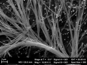
Nanowires (both CdTe and ZnO) were electrodeposited by means of template replication.
ZnO nanowires were prepared by electrochemical deposition from a simple nitrate bath. A multi-step process starting with hydroxide formation by nitrate reduction at the electrode, zinc hydroxide precipitation and finally its decomposition and consequent formation of zinc oxide leads to nanowire growth. It was found that ecellent quality nanowires with high aspect ratio are obtained for working electrode potential in the range -800 mV - -1200 mV. Structural investigations show the (200) texture for all the potential range. The optical characteristics were found to be typical for zinc oxide, reflection spectra being employed to determine the band gap value of 3.2 eV. Photo – and cathodo – luminescence show strong defect related emission and no band to band emission, meaning that the nanowires have a high defect concentration.
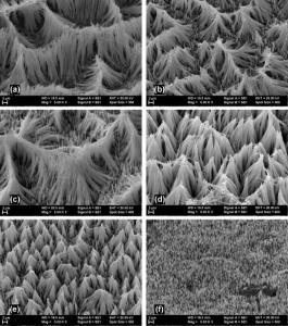
Semiconductor (ZnO) nanowires grown at different potentials by using a template approach.
Semiconductor (CdTe) nanowires grown at different potentials by using a template approach.
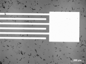
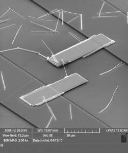
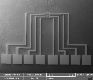
-> The nanowires were further placed on substrates with interdigitated electrodes prepared by photolithography.
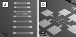
The interdigitated electrodes were fabricated on Si/SiO2 substrates.
-> Further, wires were placed onto the electrodes.
2014
Focused ion beam induced metallization (FIBIM) was employed for providing individual nanowires with electric contacts. Further, electrical measurements were performed on individual nanowires contacted in this way. The influence of a bottom gate was investigated and it was found that surface passivation leads to improved transport properties.
Further the wires were provided with individual contacts by means of electron beam lithography. It was found that for good electrical contacts, two step deposition is necessary with one of the steps taking place with a tilted sample. This addresses the problems related to the three-dimensional nature of the device. Further, a thermal annealing step at 350°C is performed, which leads to a decrease in contact resistance.
ZnO nanowire contacted by means of e-beam lithography
Besides ZnO nanowires CuO nanowires were also prepared and contacted by the method described above. In each case electrical characterization was performed.
Field effect transistor behaviour was observed for each type of nanowires when the sillicon substrate was employed as a back gate.
2015
CdTe nanowires were contacted by means of focused ion beam metallization. Field effect was demonstrated for this type of nanowires.
Electrical contacts obtained by hotolithographic process
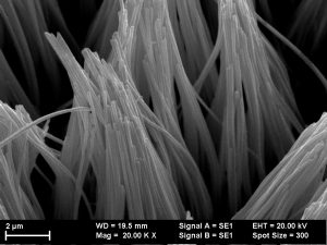
Nanowires prepared by template replication
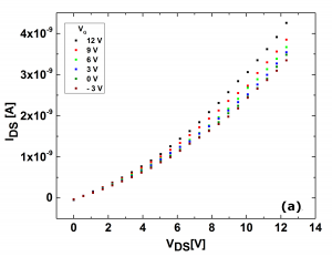
Field effect transistor behavior was emonstrated for CdTe nanowires with both uniform and modular composition
The experiments made on modulating the doping by electrodeposition potential gave the opportunity of fine tuning the transport properties.
Field Effect Transistor with Electrodeposited ZnO Nanowire Channel, Camelia Florica, E. Matei, A. Costas, M. E. Toimil Molares, I. Enculescu, Electrochimica Acta, 137, 290-297, 2014
Metallic nanowires and nanotubes prepared by template replication, E. Matei, M. Enculescu, N. Preda, Camelia Florica, A. Costas, C. Busuioc, M. E. Toimil Molares, I. Enculescu, Springer-Verlag Berlin Heidelberg 2014 V. Kuncser and L. Miu (eds.), Size Effects in Nanostructures, Springer Series in Materials Science 205, DOI 10.1007/978-3-662-44479-5_5, ISBN 978-3-662-44478-8
PROJECTS / NATIONAL PROJECTS