Acceptor removal process in irradiated p-type Silicon sensors – defect investigations and parametrization /ARP
Project Director: Dr. Ioana PINTILIE
Project ID: 08CERN/2022
Duration: 1.01.2022- 30.09.2024
Project title: Acceptor removal process in irradiated p-type Silicon sensors - defect investigations and parametrization /ARP
Project objectives:
The proposed project is embedded as part of the RD50 efforts, in the subgroup Defect and Material Characterization. The director of the present project is the leader of the NIMP team involved in the CERN-RD50 collaboration and the convener of this research line within the RD50 collaboration. The specific project proposed here is embedded as part of the RD50 efforts, in the subgroup Defect and Material Characterization. The general objective of the project is to understand the acceptor removal process in irradiated p-type silicon, parametrize it for various content of B, C and O impurities and irradiation fluences, finding this way proper defect engineering solutions to maximize the radiation hardness of different types of sensors (single pads, pixel and strips, LGAD and HVCMOS). Common for all these new sensors is the loss of initial Boron doping concentration caused by irradiation, an effect known as the acceptor removal process (ARP). During the present project the necessary defect investigation studies will be performed in order to understand the B removal in irradiated p-type silicon and provide the input defect parameters and generation rates needed for a reliable parametrization of ARP in PAD, LGAD and HVCMOS devices developed within RD50 collaboration. Previous studies revealed that several major obstacles that were preventing the achievement of enough knowledge for parametrizing the ARP and find applicable solutions to minimize this process in the devices of interest: (i) The bistability of BiOi defect, measurable in only one of the two configurations – the BiOiA(0/+), along with the long time needed for stabilizing the defect structural configuration. (ii) Impossibility of investigating the ARP in the LGADs gain layer only, after high fluences, and determine the defects depth profile caused by B and C implantations in the p+ gain layer. (iii) Impossibility of performing defect investigations in the junction between the p-substrate and deep n-well (DNWELL) layers of the HVCMOS structures fabricated so far by any of the spectroscopic techniques due to the small capacitances of the structures and small breakdown voltage. In addition, preliminary studies revealed that most often the amount of Boron in the samples is not equal with the doping extracted from CV measurements, the producers of the Si wafers achieving the required doping by using Phosphorus for compensation. This has tremendous influence on any attempt of parametrizing the ARP. The present project aims to overpass these issues by employing comprehensive studies for establishing: the impurity content in the wafers and in the implanted layers (by LA-ICPMS and SIMS investigations), the defect generation rates in the bulk and implanted layers of the structures of interest as well as the time constants for stabilizing the devices (by DLTS, TSC, CV/IV), all the parameters the ARP depends on for a reliable description of this process in PAD, LGAD and HVCMOS structures (by modelling with reliable inputs delivered by defect and impurities investigations). The ultimate goal of the project is to succeed parametrize the ARP effect for different operation scenarios and provide defect engineering optimization solutions for minimizing this detrimental effect.
Stages/Activities (Year)
I. Study of irradiated PAD and LGAD devices (2022)
I.1 LA-ICPMS studies (determination of impurity content in Si sensors)
I.2 CV/IV and defect investigations
I.3 Numerical modelling of the variation in time of IV/CV (Neff) and of the DLTS/TSC signals from BiOiA(0/+)
I.4 Develop computing models for describing the temperature dependent measured signals in highly irradiated devices
II. Further studies including G-type PAD diodes and passive HVCMOS structures (2023)
II.1 LA-ICPMS studies on as processed and as irradiated new devices
II.2 Continue the CV/IV and defect investigations, including HVCMOS test samples and not irradiated G-type diodes with different C implantations
II.3 Modelling the defect kinetics in the investigated structures
III. Parametrization of ARP in irradiated PAD, G-PAD, LGAD and HVCMOS structures (2024)
III.1 LA-ICPMS studies on irradiated and annealed G-type PAD diodes and passive HVCMOS structures
III.2 CV/IV and defect investigations on G-type PAD with different C implantations, after irradiation, annealing studies
III.3 Develop ARP model describing all the experimental results
Results
2022
The ARP project started in 2022. During this year all the research activities were performed on the irradiated PAD and LGAD devices available for being studied at the beginning of the year. In the following we will describe the achieved progress according to each of the planned activities for this first stage of the ARP project.
I. 1. LA-ICPMS studies - regarding the Boron and Phosphorous depth profiles
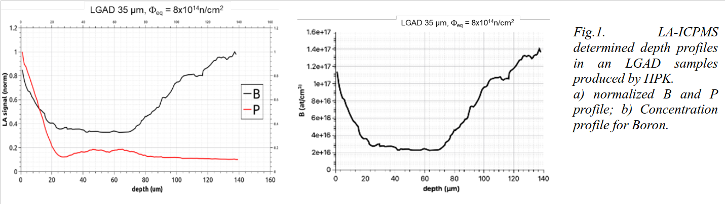
The 11B and 31P signals have been acquired in several samples. For the calibration of 11B concentration, a NIST standard (certified SRM 612) with a known concentration of 32 ppm 11B has been used. Samples have been probed in-depth using laser pulses with a fluence of 35 J/cm2, 100 μm aperture, 1 Hz probing frequency. The depth resolution of the probe was estimated by optical microscopy at 0.54 μm/pulse in NIST standard and 1.19 μm/pulse in Si samples. Examples of determined depth profiles are given in Fig. 1. Although overall the measured profiles corresponds to a LGAD structure (n++-p+-p-p++) the delimitation between the differently doped regions are far from being sharp, indicating a strong diffusion of Boron from the p++ substrate and from the P implanted n++ regions into the bulk. The bulk region with a low homogeneous B doping is of about 35 µm while the presence of P extends from 2 µm implantation layer to 20 µm in the bulk.
I. 2. CV/IV and defect investigations
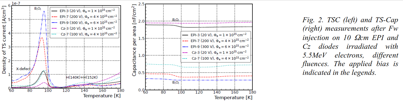
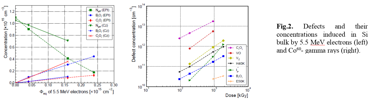
This type of investigations was systematically performed on several EPI, CZ and FZ, PAD and LGAD diodes, of different resistivity (10 cm, 50 cm, 250 cm, 1000 cm, 12 kcm) after irradiation with different particles (gammas, 5.5 MeV and 200 MeV electrons, 230 MeV and 24 GeV protons, 1 MeV neutrons), all for getting the introduction rates of Boron related defects. While all type of measurements (CV/IV, DLTS and TSC) measurements can be consistently analysed on PAD diodes, for LGADs no reliable correlation between the results of different type of measurements can be achieved. We demonstrate that while DLTS is not applicable on LGADs, the TSC measurements, although detect the radiation induced defects, are influenced by the temperature and bias dependent multiplication effect the gain layer has, making thus difficult to distinguish between signals coming from the Si bulk or from the highly doped gain layer. The solution planned in a next step is to process and characterize highly-irradiated ~ 10 cm silicon pad diodes with doping concentrations that mimic the gain layer of LGAD. Special efforts were dedicated to develop measurement procedures/techniques for quantitative defect analyses of the signals measured in highly irradiated diodes that cannot be fully depleted. We show that quantitative evaluations can be done by employing both TSC and TS-Cap (see Fig.2 for exp. data).
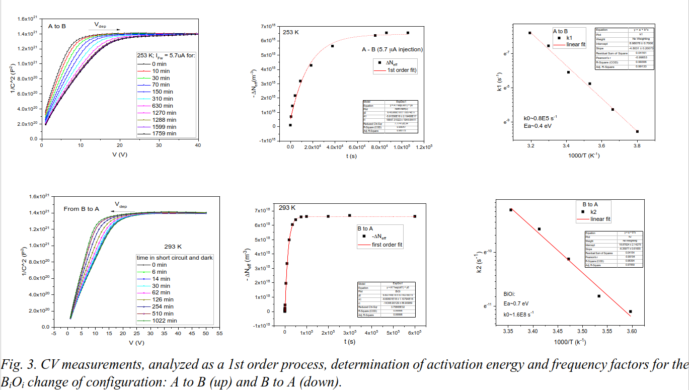
I. 3. Numerical modelling of the variation in time of IV/CV (Neff) and of the DLTS/TSC signals from BiOiA(0/+). The reversible switch between the two BiOi configurations (A and B) was investigated on a high resistivity FZ PAD diode irradiated with 1014 1 MeV neutrons/cm2. Due to the timescale involved for the processes, we monitored the change in Neff as results from CV characteristics in the 40 oC range. From changing the A (stable) to B (un-stable) configuration we used a small Fw current, similar to the photocurrent generated in short circuit by ambient light. The switch from B to A configuration, takes place slowly once the excess of carriers is removed. We have followed these processes for different temperatures between 243K and 313 K in order to extract the time constants, the corresponding activation energies and the frequency factors. A paper on this subject is under preparation.
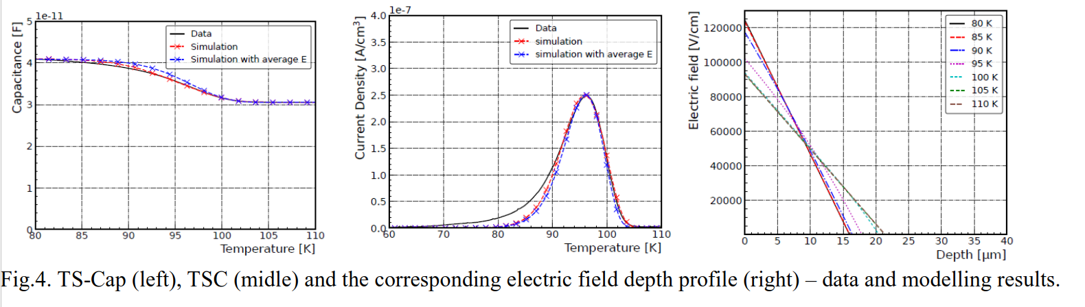
4. Develop computing models for describing the temperature dependent measured signals in highly irradiated devices. The main modelling result refers to the case of defects showing an enhanced electric field emission in highly irradiated samples when the diodes cannot be fully depleted and thus, the active volume of the samples for an applied voltage varies with temperature (decreases when electrons are emitted from defects and increases when holes are emitted). In addition, the non-homogeneous discharge of coulombic centers (as BiOi) change the local electric field (E) and this poses an additional challenge for simulating the TSC signals. As described above, we found useful in such situations to measure TS-Cap, in the same conditions as TSC. From TS-Cap one can extract the temperature dependence of the depleted thickness and account for it, beside the Poole Frenkel (PF) effect, in modelling the TSC signals. We did such simulations for fitting both TSC and TS-Cap signals, in two cases, accounting for the E depth distribution and the 3D PF effect as well as considering an average <E> when calculating the PF coulomb interaction. The modelling results along with the experimental ones are given in Fig.4. The modeling also pointed out that for low resistivity diodes, where the variation of E is large and abrupt, the approximation used in 3D PF theory (constant E over large distances around the defect) does not hold anymore – the defect rather feel an average E.
2023
The main achievements in 2023 are:
- Bistability of a Boron containing donor (BCD) - identified in the literature as BiOi or BsSii defect. The reversible switch between the two defect configurations (A and B) started to be investigated on 1 MeV neutron irradiated PAD diodes in order to extract the time constants of the defect transformations, the corresponding activation energies and the frequency factors. We found that the change from A-to-B configuration is triggered by exposing the sample to a quite small excess of carriers at temperatures close to ambient ones. From the B configuration the defect switches slowly back to A if the excess of carriers is removed.
- Analyses of impurity content. LA-ICPMS investigations on irradiated PAD and LGAD devices of different resistivities/technologies were performed for getting the profile of Boron in the devices, after irradiation and after annealing at moderate temperatures.
- Defect investigations (DLTS or TSC/TSCap in connection with CV/IV) on the already received irradiated PAD and LGAD Si sensors. While all the investigation methods can be successful applied on PAD diodes, we evidence the reasons for which the measurements on LGAD are not reliable for quantitative evaluations. We established that for an un-doubtful characterization of LGADs and further understanding the gain loss, special PAD, n+-p-p+ samples, mimicking the gain layer in the presence of different amounts of B, O, C and P impurities, has to be fabricated and studied. In this respect, we applied for a project inside RD50 and get a financial support of ~26000 EUR. Besides NIMP another 6 institutions are involved in this RD50 project, each contributing with 3500 EUR for covering the full cost of producing such samples (of 52165 EUR).
- Development computing models for describing the temperature dependent TSC/TSCap signals in highly irradiated devices- as a first attempt of determining the concentration/parameters of defects in devices that cannot be fully depleted during temperature scans. We show that in such cases, of very much interest, by combining TSC and TSCap experiments, accurate evaluations can be made.
During 2023 all the research activities were performed on the irradiated PAD and LGAD devices available at the beginning of the year (5.5 electrons, Co60 and 1 MeV neutrons). The achieved progress according to each of the planned activities for this second stage of the ARP project consists in:
1) Studies of different impurities in silicon and elaborate the strategy for fabricating specific defect engineered PAD diodes mimicking the gain layer in LGADs. Starting from LA-ICPMS and/or SIMS experiments, TCAD and SRIM simulations were performed in order to find the most appropriate co-implantations conditions of C and P in low resistivity B-doped silicon, oxygenated or not, to best mimic a defect engineered gain layer in LGADs – see Fig. 1.
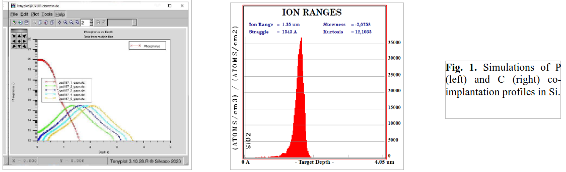
While O can be homogeneously introduced in Silicon bulk by O diffusion from the surface oxide layer, the co-doping with C and P, in the bulk, beyond the n+ (P implanted) layer has to be done by deep implantations. The simulations has shown that at least 4 deep P co-implantations are needed to get a 1.5 µm thick P partially compensated p-type silicon beyond the n+ layer. Presently, such diodes are under fabrication by CiS, Germany.
2) Macroscopic and microscopic investigations of the radiation damage induced by 5.5 electrons, Co60 and 1 MeV neutrons, in different types of diodes (EPI, FZ, Cz), with focus on the acceptor removal process (ARP). In all the cases, the loss in Neff is well described by the determined concentration of B containing donors (counted twice because they not only remove an acceptor but also create a donor instead) after irradiation and subsequent annealing treatments (Fig. 2 left). The Co60 gamma irradiations evidenced the formation of a 2nd order point defect (Ip* in Fig.2 right). Beside the experimental studies, this work also implied development of computing models for a more accurate simulation of the signals generated by radiation induced defects, especially for centers with enhanced electric field emission.
3) Defect kinetics of the bistable Boron containing donor (BCD) defect associated with ARP in irradiated p-type silicon. The bistable properties of BCD are fully reflecting in the electrical measurements performed in usual ambient laboratory conditions and they were studied in both PAD and LGAD diodes. In both type of diodes the changes in the depletion voltage are consistent with the variations of the BCD defect concentration in the A configuration, as measured with TSC. Energy barriers of 0.36 eV and 0.94 eV are determined for the A®B and B®A configurational transformations, respectively (see the configurational diagram in Fig.5).
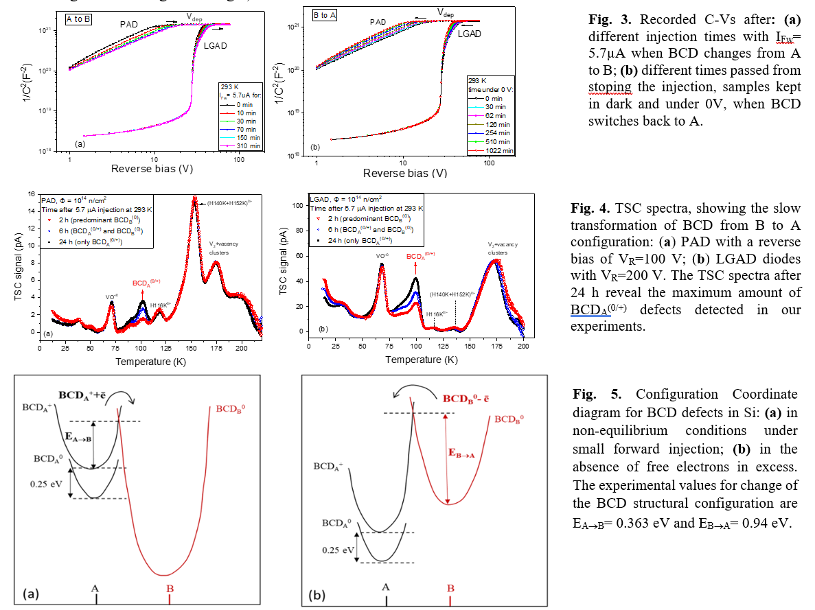
The change from A to B configuration takes place when the amount of electrons exceed the one of holes in Si bulk. For small injections conditions, as it is the case of photocurrent generated by the ambient light, such situation is encountered in a much larger volume in high resistivity samples than in the low resistivity ones. Therefore, the BCD configurational transformations are better evidenced in electrical measurements for high resistivity samples.
2024
1) „Defect characterization studies on neutron irradiated boron-doped silicon pad diodes and Low Gain Avalanche Detectors” Anja Himmerlich et al., NIMA 2023, 1048, 167977, https://doi.org/10.1016/j.nima.2022.167977 . Co-autor Ioana Pintilie: Validation, Conceptualization, Writing - Review & Editing.
2) “Investigation of the Boron removal effect induced by 5.5 MeV electrons on highly doped EPI- and Cz-silicon” C. Liao et al., NIMA 2023,1056, 168559, https://doi.org/10.1016/j.nima.2023.168559. Co-authors: Ioana Pintilie (corresponding author) - data analysis and modelling, Writing - Review & Editing, and Lucian Filip -modelling
3) “Bistable Boron-Related Defect Associated with the Acceptor Removal Process in Irradiated p-Type Silicon-Electronic Properties of Configurational Transformations”, A. Nitescu, C. Besleaga, G.A. Nemnes, I.Pintilie, Sensors 2023, 23(12), 5725; https://doi.org/10.3390/s23125725
3) “Bistable Boron-Related Defect Associated with the Acceptor Removal Process in Irradiated p-Type Silicon-Electronic Properties of Configurational Transformations”, A. Nitescu, C. Besleaga, G.A. Nemnes, I.Pintilie, Sensors 2023, 23(12), 5725; https://doi.org/10.3390/s23125725
4) “Investigation of high resistivity p-type FZ silicon diodes after 60Co γ-irradiation”, C. Liao et al., NIMA 1061, 169103, 2024, https://doi.org/10.1016/j.nima.2024.169103. Co-authors: Ioana Pintilie (corresponding author) - Conceptualization, data analysis and modelling, Writing - Review & Editing, and Andrei Nitescu – DLTS and TSC experiments and analyses.
5) “Defects and acceptor removal in 60Co γ-irradiated p-type silicon”, A. Himmerlich et al. submitted to NIMA. Co-authors: Ioana Pintilie - Conceptualization, data analysis and modelling, Writing & Editing
1) “The acceptor removal process in p-type Si sensors for future High Energy Physics Experiments – correlation with the formation of Boron related defects and their electrical activity” Cristina Besleaga (measurement and analyses), Andrei Nitescu (measurement and analyses), Lucian Filip (modelling) and Ioana Pintilie (conceptualization, supervise, establish measurement and evaluation procedures), invited talk at Global Summit on Semiconductors, Optoelectronics and Nanostructures, 23-25 of March, talk given on 23rd of March 2022 (on-line).
2) “Investigation of high resistivity p-type FZ silicon diodes after 60Co - gamma irradiation” C. Liao et al., co-author Ioana Pintilie (data analyses), 40th RD50 Workshop on Radiation hard semiconductor devices for very high luminosity colliders, 21-24 june, 2022, CERN, Geneve.
3) “Defect characterization studies on gamma-irradiated p-type Si diodes” A. Himmerlich et al., co-author Ioana Pintilie (data analyses), 40th RD50 Workshop on Radiation hard semiconductor devices for very high luminosity colliders, 21-24 june, 2022, CERN, Geneve.
4) “On the bistability of the Boron related donor associated with the acceptor removal process in irradiated p-type silicon” A. Nitescu (measurement and analyses), C. Besleaga (measurement and analyses), I. Pintilie (elaboration of measurement procedures, modelling), 40th RD50 Workshop on Radiation hard semiconductor devices for very high luminosity colliders, 21-24 june, 2022, CERN, Geneve.
5) RD50 Project proposal: Defect engineering in PAD diodes mimicking the gain layer in LGADs, Ioana Pintilie, presentation during the 40th RD50 Workshop on Radiation hard semiconductor devices for very high luminosity colliders, 21-24 june, 2022, CERN, Geneve.
6) “Defect characterization studies and modelling of defect spectra for 60Co gamma-irradiated epitaxial p-type Si diodes” A. Himmerlich et al., co-author Ioana Pintilie (data analyses) 41st RD50 Workshop on Radiation hard semiconductor devices for very high luminosity colliders, 29 Nov.-2 Dec., 2022, Sevilla, Spain.
7) “Investigation of high resistivity p-type FZ silicon diodes after 60Co - gamma irradiation” L. Chuan et al., co-author Ioana Pintilie (data analyses and modelling) 41st RD50 Workshop on Radiation hard semiconductor devices for very high luminosity colliders, 29 Nov.-2 Dec., 2022, Sevilla, Spain.
8) Bistable Boron related defect associated with the acceptor removal process in irradiated p-type silicon – electronic properties of configurational transformations, A. Nitescu, C. Besleaga, G.A. Nemnes, I.Pintilie, 42nd RD50 Workshop on Radiation Hard Semiconductor Devices for Very High Luminosity Colliders (Montenegro), 20-23 June 2023. https://indico.cern.ch/event/1270076/contributions/5450173/
9) Defect spectroscopy on 23 GeV Proton-Irradiated CZ Pad Diodes, N. Sorgenfrei, E. Fretwurst, Y. Gurimskaya, A. Himmerlich, C. Liao, M. Moll, I. Pintilie, J.Schwandt, M. Wiehe, 42nd RD50 Workshop on Radiation Hard Semiconductor Devices for Very High Luminosity Colliders (Montenegro), 20-23 June 2023. https://indico.cern.ch/event/1270076/contributions/5450169/
10) On-going studies on diminishing the acceptor removal effect by tuning the charge state of Boron containing defects in p-type irradiated PAD samples, A. Nitescu, L.D. Filip, C. Besleaga, G.A. Nemnes, I.Pintilie, 1st DRD3 Workshop (CERN, Geneve), 17-21 June 2024. https://indico.cern.ch/event/1402825/contributions/5998116/
PROJECTS/ NATIONAL PROJECTS
Copyright © 2025 National Institute of Materials Physics. All Rights Reserved