Title: “Multifunctional optoelectrical sensor based on two-dimensional MoS2 atomically thin layers grown by selective nucleation”
Acronym: 2Doptosens
Project ID: PN-III-P2-2_1-PED-2021-2457
Project Director: Dr. Toma Stoica
Project Type: National
Program: Program 4 – Basic and Frontier Research: Complex Projects of Frontier Research
Funding Agency: Unitatea Executiva pentru Finantarea Invatamantului Superior, a Cercetarii, Dezvoltarii si Inovarii - UEFISCDI
Contractor: NATIONAL INSTITUTE OF MATERIALS PHYSICS (INSTITUTUL NATIONAL DE CERCETARE - DEZVOLTARE PENTRU FIZICA MATERIALELOR)
Status: In progress
Starting Date: 24/06/2022
Ending Date: 31/07/2024
Summary:
Optoelectrical multifunctional sensors will be obtained based on selective nucleation and growth of two-dimensional 2D-MoS2 atomically thin layers on SiO2/Si patterned substrates, by using Physical Vapor Deposition method. The substrate patterning will be performed by deposition of Mo pads before growth of MoS2 flakes. The precise localization of selectively grown 2D-MoS2 flakes allows the fabrication of the optoelectrical sensors by deposition of metallic contacts using photolithographic technique with alignment to the patterns of the substrate. The atomically thin 2D-MoS2 layers are very sensitive to external excitation as for example light illumination or adsorbed molecules on the 2D-MoS2 free layer surface. Using the Si substrate as gate electrode, the (photo)sensitivity of the device can be controlled and enhanced by field effect. Based on the high sensitivity expressed by electric and photoelectric behaviour, the 2D-MoS2 optoelectrical sensors are recommended for many practical applications, as for example biosensors (protein detection, DNA compatibility, acetone in human breath for diabetes, etc) and chemical sensors for pollution monitoring. The validation of the optoelectrical sensor demonstrator in this project according to TRL 3 includes the testing experiments on spectral photocurrent, as well as on electrostatic doping in 2D-MoS2 layers by field effect and adsorbed acetone molecules.
Dr. Toma Stoica (https://www.brainmap.ro/toma-stoica) - Principal Investigator
Dr. Ciurea Lidia Magdalena (https://www.brainmap.ro/lidia-magdalena-ciurea)
Dr. Ionel Stavarache (https://www.brainmap.ro/ionel-stavarache)
Dr. Adrian Slav (https://www.brainmap.ro/adrian-slav)
Dr. Ana-Maria Lepadatu (https://www.brainmap.ro/ana-maria-lepadatu)
Dr. Elena Matei ( https://www.brainmap.ro/elena-matei)
Dr. Catalin Palade (https://www.brainmap.ro/catalin-palade)
Dr. Ioana Maria Avram Dascalescu (https://www.brainmap.ro/ioana-maria-dascalescu)
PhD Student Ovidiu Cojocaru (https://www.brainmap.ro/ovidiu-cojocaru)
SUMMARY OF STAGE 1
The goal of the 2DOPTOSENS project is the manufacture of multifunctional optoelectric sensors obtained by nucleation and selective growth of 2D-MoS2 thin layers on structured SiO2/Si substrates by Physical Vapor Deposition (PVD) method.
Stage 1/2022 has as a main objective the preparation of the conditions for carrying out selective depositions of 2D-MoS2 and for the manufacture of optoelectronic devices in the following stages, through studies on the operating parameters of the 2D-MoS2 reactor and obtaining test samples of depositions on structured supports, as well as photolithographic mask design. This objective was achieved through the activities proposed for Stage 1 of the Implementation Plan: ● Calibration of the operating parameters of the 2D-MoS2 reactor; ● PVD growth of 2D-MoS2 on test substrates; ● Statistical characterization of 2D-MoS2 growth; ● Morphological and structural characterization; ● Creation of the project web page and permanent updating.
In this Stage, experiments were carried out to find out the operating parameters of the equipment, the performances of the depositions on structured and unstructured substrates that led to the in-depth understanding of the processes involved in these growths of 2D-MoS2 layers and the establishment of measures to improve the depositions and their characterization. First of all, the parameters and operating conditions of the installation and the deposition process were investigated and improvements were made, reducing the leakage rate by over an order of magnitude. The thermogravimetry measurements showed the stability of the MoS2 powder up to 1100oC in the inert atmosphere, but also its oxidation at over 500oC in the atmosphere containing oxygen, thus demonstrating the importance of reducing traces of oxygen in the working atmosphere, the exchange reaction of replacing S by O being stronger the higher the oxygen partial pressure and the higher the temperature. The temperature gradient in the oven inside the tube was calibrated in order to evaluate the temperature of the samples during deposition. The composition and crystalline quality of the MoS2 source was tested by Raman scattering measurements. A number of 10 test depositions of 2D-MoS2 were carried out, varying various parameters such as the temperatures set in the three zones of the furnace (the temperature of the MoS2 powder set between 970oC and 1050oC), the duration of the deposition (30 – 720 min), the flow of Ar (36 – 144 sccm) and working pressure (10 – 27 mbar). 1x1 cm2 SiO2/Si substrates with ~300nm thick SiO2 layer were used, either structured with SiO2 windows obtained by chemical etching in HF, or unstructured.
The statistics on a number of 12-18 samples/deposition of the selective growths by nucleation in the SiO2 windows, as well as at the edge of the samples, was investigated by optical microscopy. The temperature gradient achieved in the three-zone furnace ensures lower deposition temperatures the more the samples were located at greater distances from the hottest zone where the MoS2 powder was placed. Consistent selective deposits are observed from 10 cm to 25 cm away from the source of MoS2 at temperatures below 800oC and above 630oC. The zone of maximum efficiency of the deposition expands and moves slightly when the flow of Ar increases and the working pressure decreases. Raman scattering measurements showed that traces of oxygen in the working atmosphere have the effect of oxidizing the MoS2 deposits and transforming them into monoclinic MoO2. By reducing the vacuum leaks, selective depositions of non-oxidized crystalline MoS2 were obtained. In this stage, deposition tests were also carried out using supports structured by the deposition of metallic Mo strips, which showed the accumulation of MoS2 deposited at the edge of these strips. In order to increase the efficiency and quality of the 2D-MoS2 deposits, the temperature gradient and the limit vacuum will be increased in the future. For the next stages, photolithographic masks were designed for structuring the supports before the depositions and the electrodes of the devices for opoelectronic measurements.
In conclusion, the objectives and activities proposed for Stage 1/2022 were fully achieved.
SUMMARY STAGE 2
The project goal of 2DOPTOSENS project is to fabricate multifunctional optoelectronic sensors through selective growth of thin 2D-MoS2 layers on structured Mo/SiO2/Si substrates. The main objective of Stage 2/2023 is selective growth of 2D-MoS2 and the fabrication of optoelectronic samples. To achieve the goals of Phase 2, the following activities were carried out as provided in the Implementation Plan: ● Fabrication of structured substrates; ● Selective growth of 2D-MoS2 on structured substrates; ● Investigations of morphology and crystalline structure of the selective 2D-MoS2 growths; ● Fabrication and optimization of optoelectronic test samples – Part I; ● Dissemination of results and updating the project's website.
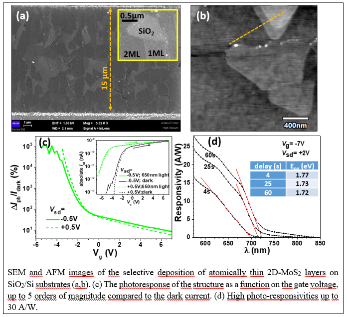
The activities in this Phase 2/2023 focused on achieving high-quality selective depositions on SiO2/Si substrates with a structured Mo layer. The first activity involved making improvements to the deposition installation: better isolation between furnace zones, a better degassing vacuum using a turbo pump, and improved sealing. Another practical activity for achieving the phase objectives was manufacturing photolithographic masks and samples with a structured Mo layer using photolithography. Selective depositions were obtained by the PVD of 2D-MoS2 close to Mo pads, extending up to 160 µm from Mo, with decreasing thickness down to 1-2 MLs. A critical analysis of the PVD deposition mechanism using MoS2 powder as a precursor showed that the basic mechanism is not well established in the literature, with the PVD process possibly involving CVT (chemical vapor transport), as well as Mo-CVD, a deposition using oxidized Mo and sulfur vapors as precursors. Mo-CVD resulted in selective depositions restricted to the immediate vicinity and in contact with Mo pads. Good results were obtained using substrates structured with naturally oxidized Mo. It was found that the native oxide is sufficient to lead to selective 2D MoS2 depositions filling the gap between Mo electrodes from 5 µm to 20 µm wide. SEM and AFM measurements showed these depositions consist of MoS2 plates (flakes) with thicknesses of 4 nm (6 MLs) in the 5 µm gap, and only 1 – 2 MLs in gaps of 15 µm and 20 µm. The selective depositions thus obtained using substrates with Mo "finger contacts" geometry structures could be used to fabricate field-effect devices directly from the deposited samples, by contacting the large pads of the structures, serving as source-drain electrodes, and the doped Si substrate as the gate electrode. Multiple characterization tests/measurements were conducted on these devices. In these devices, the dark current dramatically reduces by nearly 5 orders of magnitude when changing the gate voltage from +7V to -7V, demonstrating the n-type semiconductor nature of the 2D MoS2 layers. Relative photosensitivity of the order of 105(%) was achieved by monochromatic illumination of 4.5x10⁻⁴ mW/cm2 at 650 nm. The spectral responsivity of 15 – 25 A/W at 600 nm wavelength showed a photosensitivity threshold at 1.72 – 1.77 eV corresponding to 2 MLs MoS2 thickness.
The web page of the 2DOPTOSENS project has been updated: https://infim.ro/en/project/multifunctional-optoelectrical-sensor-based-on-two-dimensional-mos2-atomically-thin-layers-grown-by-selective-nucleation/.
In conclusion, the objectives and activities proposed for Stage 2/2023 were fully achieved.
SUMMARY STAGE 3
The aim of the 2DOPTOSENS project is the fabrication of multifunctional optoelectric sensors obtained by selective growth of 2D-MoS2 thin layers on structured Mo/SiO2/Si substrates.
Stage 3/2024 has as its main objective Manufacturing and functional tests of optoelectric sensors. To achieve the objectives of Stage 3, the following activities provided for in the Implementation Plan were carried out: ● Manufacture and optimization of optoelectric test samples – part II; ● Testing the sensitivity of optoelectric samples to external stimuli; ● Functional testing of the demonstrator and evaluation of operating parameters at TRL3 level; ● Updating and finalizing the project web page; ● Dissemination of results through presentation at conferences, ISI paper and patent application. The activities of this Stage 3/2024 aimed primarily at the optimization of the Mo-CVD method of selective deposition of 2D-MoS2 between Mo electrodes for the facile fabrication of field-effect devices sensitive to various stimuli. The 2D-MoS2 layers selectively grown by this method consist of interconnected flakes of various thicknesses (generally from 1 monolayer to 4 atomic monolayers), their density and thickness distribution varying depending on the gap width between the Mo electrodes that served to selective growth. A total of 14 deposition were made, the fabrication process being described in detail. The aim was to optimize the selectivity and reproducibility of the selective growth of 2D-MoS2 layers for structures with various distances between electrodes. Morphology and structure studies were done, especially by optical microscopy and Raman spectroscopy. Massive selective increases covering all Mo electrode gaps up to 20 µm were obtained by increasing the deposition temperature from 750 oC to 770 oC. Analysis of the selective growth as a function of the distance from the edge of a large pad extended the selective growth up to 15 µm, as well as the occurrence of a deposition beyond this zone consisting of small and dense islands of monolayer thickness. The fabrication of the selectively grown 2D-MoS2-based field-effect optoelectric device is described in conjunction with functional tests. The structures most sensitive to stimuli such as light, gate voltage and the adsorption of gas molecules were those with a wider gap between the electrodes, of 15 µm and 20 µm, which we will designate as #15 µm and #20 µm samples, respectively. In this Stage 3, we focused on studying the response of the devices to the adsorption of polar molecules, especially to water in air and acetone vapors. It could thus be seen that the samples are very sensitive to the measurement atmosphere in air at atmospheric pressure and in vacuum, the dark current increases in high vacuum in both structures by a factor of 2.4–2.6, compared to that at atmospheric pressure. Molecule adsorption sensitivity tests were the basis for defining the TRL3 demonstrator of this project. The response of the devices to external stimuli depends on the average value and the distribution of the thicknesses of the flakes in the 2D-MoS2 layer, which depends on the value of the gap. Thus, the spectral photoconductivity at #20µm increases in high vacuum by a factor of 2.1, which adds to the dark current increase resulting in a total current increase factor of over 4.5. At #15µm, the spectral photoconduction does not change significantly at high vacuum, only the total current. The dramatic decrease in current at atmospheric pressure is due to the adsorption of H2O molecules.
The web page of the 2DOPTOSENS project has been updated: https://infim.ro/en/project/multifunctional-optoelectrical-sensor-based-on-two-dimensional-mos2-atomically-thin-layers-grown-by-selective-nucleation/.
In conclusion, the objectives and activities proposed for Stage 3/2024 were fully achieved.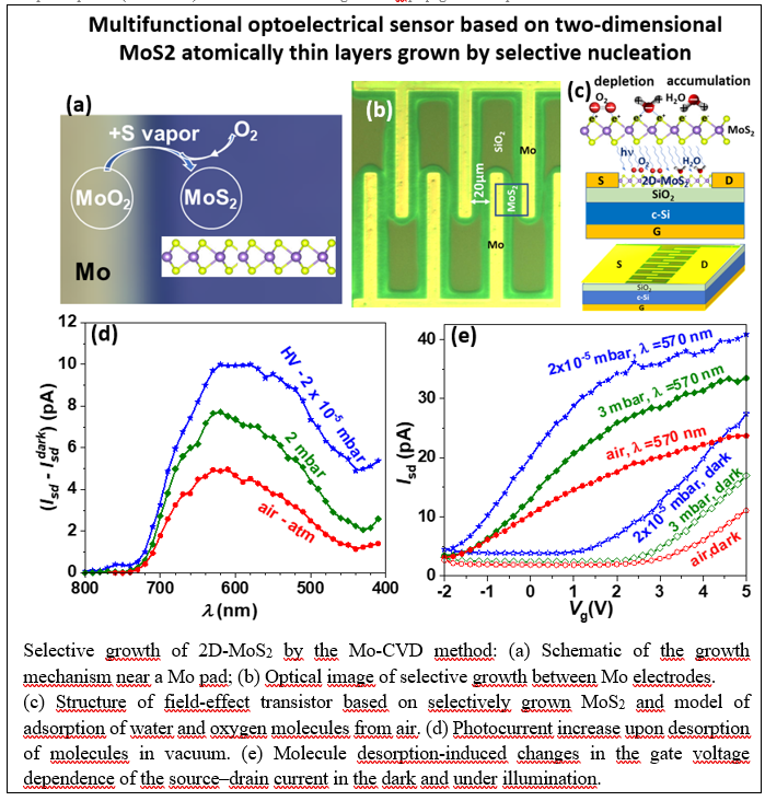
Articles published in ISI-quoted journals
- “Selectively grown 2D-MoS2 for molecule adsorption-sensitive field-effect structures”, autori: I. Stavarache, C. Palade, A. Slav, I. Dascalescu, A.-M. Lepadatu, E. Matei, C. Besleaga, M. L. Ciurea, B. E. Kardynal, Toma Stoica, summitted to ACS Appl. Nano Mater.
- "Atomically thin MoS2 layers selectively grown on Mo patterned substrates for field effect controlled photosensors", I. Stavarache, C. Palade, A. Slav, I. Dascalescu, A.-M. Lepadatu, L. Trupina, E. Matei, M. L. Ciurea, T. Stoica, ACS Appl. Nano Mater. 2024, 7, 5, 5051–5062.
Patent application
- OSIM patent application no. A/00272 (May 27th 2024) „Structură cu strat 2D-MoS2 crescut selectiv sensibilă la vapori de acetonă și procedeu de obtinere a acesteia” („Structure with selectively grown 2D-MoS2 layer sensitive to acetone vapor and method of obtaining it”), T. Stoica, I. Stavarache, C. Palade, A. Slav, I. M. Dascalescu, A.M. Lepadatu, M.L. Ciurea
International Conference presentations
- Presentation:: "2D-MoS2 selectively grown on the Mo patterned substrates for photosensitive field effect transistor",
I. Stavarache, C. Palade, A. Slav, I. Dascalescu, A.-M. Lepadatu, L. Trupina,E. Matei, M. L. Ciurea, T. Stoica,
ROCAM X Jubilee Conference, 15–18 July 2024, Bucharest, Romania - Presentation: "Vapor transport growth of localized atomically thin 2D-MoS2 layers",
I. Stavarache, C. Palade, A. Slav, I. Dascalescu, A.-M. Lepadatu, E. Matei, M. L. Ciurea, T. Stoica
International Semiconductor Conference, 11–13 October 2023, Sinaia, Romania
Project Contact Person:
Project Director: Dr.Toma Stoica
National Institute of Materials Physics, Atomistilor 405A., 077125 Magurele - Bucharest, ROMANIA
Tel:+40--(0)21-2418-171
Email: toma.stoica@infim .ro
PROJECTS / NATIONAL PROJECTS