High photoconductive oxide films functionalized with GeSi nanoparticles for environmental applications, PhotoNanoP
Project Director: Dr. Magdalena Lidia CIUREA
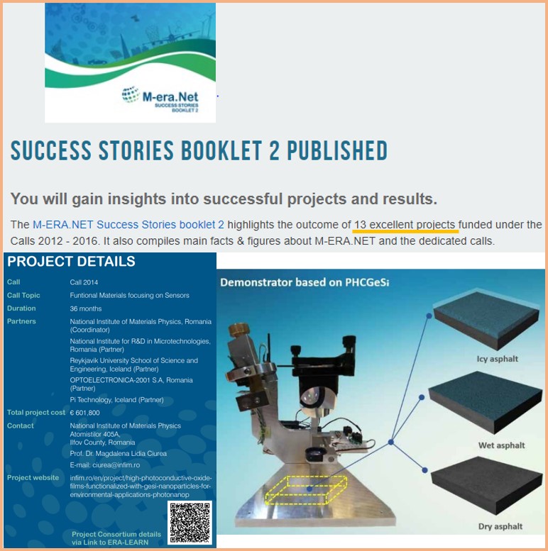
The goal of this project is obtaining oxide films (TiO2, SiO2) functionalized with embedded GeSi NPs, having good photoconductive properties in VIS-NIR for optical sensors to be used in environmental applications, to evaluate the slippery road conditions causing traffic accidents by spectrally discriminating between dry, wet and icy road surfaces to enhance collision avoidance. These films have selective spectral sensitivity in the ranges of reflection/ absorption bands of dry, wet and icy asphalt, and consequently can discriminate between these different road conditions.
The project will be accomplished by the consortium formed of National Institute of Materials Physics (Project Coordinator, P1), National Institute for R&D in Microtechnologies (P2), Reykjavik University School of Science and Engineering (P3) and companies OPTOELECTRONICA-2001 S.A (P4) and Pi Technology (P5).
Coordinator: National Institute of Materials Physics, Romania - NIMP
Project Coordinator: Dr. Magdalena Lidia Ciurea
Partner: National Institute for R&D in Microtechnologies, Romania- IMT Bucharest
Responsible of IMT Bucharest: Dr. Adrian Miron Dinescu
Partner: Reykjavik University (School of Science and Engineering), Iceland - RU-SSE
Responsible of RU-SSE: Dr. Halldor G. Svavarsson
Partner: OPTOELECTRONICA- 2001 S.A, Romania - OPTOEL
Responsible of OPTOEL: Dr. Alexandra Enuica
Partner: Pi Technology, Iceland
Responsible of Pi Technology: Eng. Baldur Thorgilsson

ABSTRACT
The project PhotoNanoP, aims to obtain oxides films (SiO2, TiO2), functionalized with GeSi nanoparticles/nanocrystals (NP/NC), having photoconduction properties for environmental applications (spectral sensitivity in 0.6 – 1.2 μm range). For demonstrating the project concept, we fabricated a demonstrator (optical sensor) which is able to discriminate between different slippery conditions of the road, i.e. wet asphalt, icy asphalt and dry asphalt.
The Romanian contract between the Romanian partners has run in the period 2016 -2018, and was carried out by the consortium of •INCDFM – Project Coordinator; •IMT-Bucharest – Partner 1 and •OPTOEL 2001 SA – Partner 2.
The project has the following objectives: ● functionalizing the oxides films of SiO2, TiO2 with GeSi NP by using different deposition methods i.e. magnetron sputtering (MS), high-power impulse MS (HiPIMS) followed by subsequent thermal annealing for GeSi Np/NC formation; ● obtaining functionalized films with good photoconductive properties (PHC) by adjusting the morphology and structure by using optimization of composition and preparation parameters; ● obtaining PHCGeSi films with good photoconductive properties in the spectral range of 0.6 – 1.2 μm.; the PHCGeSi films obtained in the project are new and innovative materials.
These objectives are detailed as follows: Deposition of GeSi-SiO2 and GeSi-TiO2 films and their functionalization by embedding GeSi NPs (nanostructuring the films); u correlation between technological parameters with structure and morphology results at different stages; u developing an original model for conductivity and fototransport in functionalized oxides films for predicting the spectral sensitivity; finding the key materials parameters by atomistic simulation; u model validation by complex experimental investigations; u fabrication of test samples (optical sensor) based on functionalized films with targeted PHC properties (spectral sensitivity in 0.6 – 1.2 μm range); u innovative concept validation of the project by demonstrator (optical sensor) fabrication according with TRL 5; u dissemination and results exploitation by publishing ISI papers and presentations at prestigious international conferences, 1 patent application, 2 workshops, by taking into accounts IPRs; u coordination of joint research and pursuing objectives achievements; progress monitoring; ensuring the continuity information flow during the development of the project.
For accomplishing the PhotoNanoP project objectives like obtaining the SiO2 or TiO2 films functionalized with GexSi1-x NCs with different x compositions, we prepared and characterized two type of structures, GeSi NCs embedded in TiO2 (GeSi-TiO2 NCs) and GeSi-SiO2 NCs.
The GeSi NCs embedded in SiO2 and test structures based on them, were deposited by MS co-deposition from Ge, Si and SiO2 targets, in DC (Ge, Si) and RF (SiO2) regime, on oxidized Si substrate (by rapid thermal oxidation - RTO). After deposition, the structures were rapid thermally annealed (RTA) for nanostructuring. The structures with the best electrical and photoconductive properties are the structures with GeSi:SiO2 composition of 45%:55%:50% and RTA annealed at 800 oC. The transmission electron microscopy (TEM) evidenced the formation of GeSi NCs with diameters of 4 – 6 nm, with high density, embedded in SiO2 in a region located at the bottom of the film, while the in the middle region, the GeSi NCs have increasing diameters from the interface with the bottom region to the free surface of the film. The free surface region is amorphous and does not contain GeSi NCs. The spectral dependence of the photocurrent measured on these films (GeSi (45:55%) – SiO2 (50%)) shows very good photoconductive properties at room temperature, the edge from the long wavelengths being ~1350 nm. By decreasing the measurement temperature, the photosensitivity of the structures expands to near infrared (NIR) so that at 100 K the films are photosensitive up to 1500 – 1600 nm. These structures with optimized properties (PHCGeSi) were used for demonstrator fabrication.
The GeSi NCs embedded in TiO2 and test structures based on them, were realized in a similar way, but using specific process parameters. Besides the film structures, a multilayer structure of TiO2/(GeSi/TiO2)n/p-Si with n = 3 or 6 were deposited, too. The structure and morphology investigations (TEM, Raman and XRD) on GeSi-TiO2 NCs RTA annealed at 800 oC, evidence the formation of NCs with high concentration of Ge. The current – voltage (I-V) characteristics show linear behaviour due to high Ge concentration (GeSi NC with Ge excess in the middle of the films and high GeSi NCs concentration at the film bottom) and current – temperature (I-T) characteristics show at low temperature a I ~ exp((–T0/T)1/2 dependence that describes the electrons tunnelling between neighbour NCs. The spectral dependence of the photocurrent was measured at room temperature and at low temperatures of 100 K for different applied voltages. At 300 K, the spectral dependence evidences two maxima located at 960 nm (the main maximum) and at 730 – 740 nm, while the results obtained at 100 K show that the samples are photosensitive in NIR, in the spectral range of 1100 – 1500 nm. The photoconductive edge at long wavelengths of ~1650 nm together with GeSi NCs with Ge excess are in a good agreement with the results obtained from structure and morphology investigations.
Both structures based on GeSi-SiO2 NC and GeSi-TiO2 NC have suitable parameters for using them at the fabrication of the demonstrator – optical sensor, having high sensitivity in NIR in the spectral range of 0.6 – 1.2 μm. Together with the economic partner we fabricate the demonstrator and we tested his functionality using the KNN algorithm. From these tests we have conclude that the functional parameters of the demonstrator are in good agreement with TRL 5.
The demonstrator with targeted parameters is able to discriminate between different slippery conditions of the road, i.e. wet asphalt, icy asphalt and dry asphalt and consequently to reduce the number of car crash accidents.
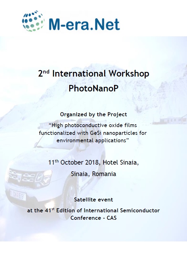
We organized the “1st International Workshop PhotoNanoP” and “2nd International Workshop PhotoNanoP” in 2017 and 2018, as a satelitte event at IEEE CAS 2018 International Conference http://www.imt.ro/cas/ in 2017 and 2018.
The scientific and technical results obtained were published in 9 ISI papers and disseminated in 10 communications at the prestigious international conferences, and 2 OSIM patent application were submitted.
In conclusion, the objectives and activities proposed to be achieved in the project were fully accomplished and the obtained results are in line with those proposed in the project.
Stage III:
The Stage III of the running project PhotoNanoP has the following scientific objectives:
- obtaining oxides films of SiO2 and/or TiO2 with GeSi NCs included in and preparing test structures based on them;
- complex characterization of the films and test structures: morphology, structure and transport properties in dark and under the illumination (these 2 objectives were reached over 2 stages in order to fulfill the targeted properties and therefore of proper technological parameters);
- selection of the samples with targeted properties for the demonstrator fabrication;
- fabrication and functional testing of the demonstrator.
In order to achieve the first two objectives (Stage II and III), the test structure based on GeSi nanocrystals (NCs) embedded in TiO2 and SiO2 were further fabricated. The GeSi-TiO2 and GeSi-SiO2 films were deposited by magnetron sputtering from three targets of Ge, Si and TiO2 or SiO2 on Si substrate, followed by rapid thermal annealing (RTA). Also, the multilayer structure of TiO2/(GeSi/TiO2)n/p-Si with n = 3 or 6 were deposited. The test structures were complex characterized by studying structure, morphological, electrical and photoconductive properties. Thus, the current-voltage (I-V) in dark and under the illumination and also the spectral dependence of the photocurrent was measured. We selected the samples with optimal parameters, that we have defined as PHCGeSi films for the fabrication of demonstrator. Both structures based on GeSi NCs embedded in TiO2 and in SiO2 have the targeted parameters for the demonstrator fabrication i.e. the optical sensor with high sensitivity in NIR, in the range 0.6 – 1.2 μm. Together with the economic partner we have fabricated the demonstrator and have performed functional tests according to TRL 5.
The demonstrator with targeted parameters is able to discriminate between different slippery conditions of the road, i.e. wet asphalt, icy asphalt and dry asphalt and consequently to reduce the number of car crash accidents.
In this stage the “2nd International Workshop PhotoNanoP” was organized as a satellite event at the IEEE CAS 2018 International Conference http://www.imt.ro/cas/.
The scientific and technical results obtained in this stage were published in 6 ISI papers, disseminated in 4 communications at the prestigious international conferences and 1 patent application was submitted to OSIM.
The project web-page was continuously updated and finalized at the same time with the PhotoNanoP project.http://infim.ro/en/project/high-photoconductive-oxide-films-functionalized-with-gesi-nanoparticles-for-environmental-applications-photonanop/
In conclusion, the objectives and activities proposed to be achieved in the Stage III/2018 were fully accomplished and the obtained results are in line with those proposed in the project.
Stage II:
The achieved results exceed the expected results for Stage II (stipulated in the Work Plan):
- process parameters for deposition and functionalization of films with GeSi nanoparticles
- morphology and structure results
- 2 sets of masks
- 4 papers published / submitted for publication in ISI journals:
1. "Photo-sensitive Ge nanocrystal based films controlled by substrate deposition temperature”, I. Stavarache, V.A. Maraloiu, C. Negrila, P. Prepelita, I. Gruia, G. Iordache, Semicond. Sci. Technol. 32 (2017), 105003.
2. "Dense Ge nanocrystals embedded in TiO2 with exponentially increased photoconduction by field effect”, A.-M. Lepadatu, A. Slav, C. Palade, V.S. Teodorescu, M. Enculescu, S. Iftimie, S. Lazanu, M.L. Ciurea, T. Stoica, submitted for publication in Scientific Reports.
3. "Influence of preparation conditions on structure and photosensing properties of GeSi/TiO2 multilayers", A. Slav, C. Palade, I. Stavarache, V.S. Teodorescu, M.L. Ciurea, R. Müller, A. Dinescu, M.T. Sultan, A. Manolescu, J.T. Gudmundsson, H.G. Svavarsson, IEEE International Semiconductor Conference - CAS Proceedings (2017), pp. 63–66.
4. "Photosensitive GeSi/TiO2 multilayers in VIS-NIR", C. Palade, I. Dascalescu, A. Slav, A.M. Lepadatu, S. Lazanu, T. Stoica, V.S. Teodorescu, M.L. Ciurea, F. Comanescu, R. Müller, A. Dinescu, A. Enuica, IEEE CAS Proceedings (2017), pp. 67–70.
- 5 conference papers:
1. "Influence of preparation conditions on structure and photosensing properties of GeSi/TiO2 multilayers", A. Slav, C. Palade, I. Stavarache, V.S. Teodorescu, M.L. Ciurea, R. Müller, A. Dinescu, M.T. Sultan, A. Manolescu, J.T. Gudmundsson, H.G. Svavarsson, IEEE International Semiconductor Conference - CAS 2017, October 11-14, Sinaia (oral presentation)
2. "Photosensitive GeSi/TiO2 multilayers in VIS-NIR", C. Palade, I. Dascalescu, A. Slav, A.M. Lepadatu, S. Lazanu, T. Stoica, V.S. Teodorescu, M.L. Ciurea, F. Comanescu, R. Müller, A. Dinescu, A. Enuica - CAS 2017, October 11-14, Sinaia (oral presentation)
3. "Ge nanocrystals in oxides with memory and photoelectrical properties", C. Palade, A. Slav, A.-M. Lepadatu, A.V. Maraloiu, S. Lazanu, C. Logofatu, T. Stoica, V.S. Teodorescu, M.L. Ciurea, The 9th International Conference on Advanced Materials - ROCAM 2017, July 11-14, Bucuresti (oral presentation)
4. "Active materials based on Ge nanocrystals in oxides for trilayer memory capacitors and photosensitive structures", A. Slav, C. Palade, A.M. Lepadatu, A.V. Maraloiu, C. Logofatu,S. Lazanu, T. Stoica, V.S. Teodorescu, M.L. Ciurea, IBWAP 2017, July 11-14, Constanta (poster)
5. "Photoconductive TiO2 films functionalized with Si(1-x)Gex nanoparticles", M.T. Sultan, J.T. Gudmundsson, M.L. Ciurea, H.G. Svavarsson, DINAMO 2017 in ICELAND, May 14-19, Siglufjordur, Iceland (poster)
- 1 patent application:
“Structuri fotosensibile pe baza de nanocristale de germaniu imersate in dioxid de siliciu pentru fotodetectori si procedeul de realizare a acestora”/ “Photosensitive structures based on Ge nanocrystals embedded in silicon dioxide for photodetectors and fabrication procedure for them”, I. Stavarache, M.L. Ciurea, V.S. Teodorescu, V.A. Maraloiu, patent application no. A 00069/09.02.2017 filled at OSIM
Project Meeting:
Meeting held on September 6-8, 2017 at RU-SSE premises in Reykjavik, Iceland.
Project Workshop:
„1st International Workshop PhotoNanoP”, Satellite event at the 40th Edition of IEEE International Semiconductor Conference – CAS 2017 (http://www.imt.ro/cas/), 12 octombrie 2017, Hotel Sinaia, Sinaia, Romania
Project web page:
Project web page http://infim.ro/en/project/high-photoconductive-oxide-films-functionalized-with-gesi-nanoparticles-for-environmental-applications-photonanop/ was updated.
Stage I:
The expected results for Stage I, in accordance with the work plan were achieved:
- process parameters for deposition of TiO2, SiO2 stoichiometric films;
- process parameters for functionalization of oxide films with GeSi NPs embedded in by RTA ;
- preliminary tests and analysis of films morphology and structure.
- 1 conference paper:
“Ge quantum dots embedded in TiO2 for VIS-NIR photodetectors”,
A.-M. Lepadatu, A. Slav, C. Palade, S. Lazanu, M. Enculescu, V.S. Teodorescu, T. Stoica, M. L. Ciurea, A. Manolescu, H.G. Svavarsson, PM-5 2016, November 10-11, Bucuresti (oral presentation)
- 1 paper for publication in ISI journal being finalized:
“Photosensing of Ge nanocrystals in TiO2 assisted by surface photovoltage”
A.-M. Lepadatu, A. Slav, C. Palade, V.S. Teodorescu, M. Enculescu, S. Lazanu, M.L. Ciurea, T. Stoica
- 1 patent application partially supported by project:
“Structuri fotosensibile pe baza de nanocristale de germaniu imersate in dioxid de siliciu pentru fotodetectori si procedeul de realizare a acestora”/ “Photosensitive structures based on Ge nanocrystals embedded in silicon dioxide for photodetectors and fabrication procedure for them”
I. Stavarache, M.L. Ciurea, V.S. Teodorescu, V.A. Maraloiu, being finalized, to be filled at OSIM
Kick-off meeting:
The meeting for organization and correlation of all activities that will be carried out by all project partners was held on Skype on April 25 2016 after each partner teams organized and planned their own activities. The Romanian partners met at NIMP premises, while the Islandic partners met at Reykjavik University.
Project web page: http://infim.ro/en/project/high-photoconductive-oxide-films-functionalized-with-gesi-nanoparticles-for-environmental-applications-photonanop/
Project web page was created and updated.
Research stages
- Working visit of PhD student Muhammad Taha Sultan (RU-SSE) at NIMP, between 23th June and 11th July: preparation of test samples; electrical and photoelectrical measurements on NIMP and RU-SSE test samples within PhotoNanoP research project
- papers published in ISI journals:
- “GeSi nanocrystals photo-sensors for optical detection of slippery road conditions combining two classification algorithms”, C. Palade, I. Stavarache, T. Stoica, M. L. Ciurea, Sensors 20, 6395 (2020).
- “SiGe nanocrystals in SiO2 with high photosensitivity from visible to short-wave infrared”, I. Stavarache, C. Logofatu, M. T. Sultan, A. Manolescu, H. G. Svavarsson, V.S. Teodorescu, M. L. Ciurea, Sci. Rep. 10, 3252 (2020).
- “Obtaining SiGe nanocrystallites between crystalline TiO2 layers by HiPIMS without annealing”, M. T. Sultan, J. T. Gudmundsson, A. Manolescu, V. S. Teodorescu, M. L. Ciurea, H. G. Svavarsson, Appl. Surf. Sci. 511, 145552 (2020).
- “Ge nanoparticles in SiO2 for near infrared photodetectors with high performance”, I. Stavarache, V. S. Teodorescu, P. Prepelita, C. Logofatu, M. L. Ciurea, Sci. Rep. 9, 10286 (2019).
- “Efficacy of annealing and fabrication parameters on photo-response of SiGe in TiO2 matrix”, M. T. Sultan, J. T. Gudmundsson, A. Manolescu, V. Teodorescu, M. L. Ciurea, H. G. Svavarsson, Nanotechnology 30, 365604 (2019).
- “Fabrication and characterization of Si1-xGex nanocrystals in as-grown and annealed structures: A comparative study”, M. T. Sultan, V. S. Teodorescu, J. T. Guðmundsson, A. Manolescu, M. L. Ciurea, H. G. Svavarsson, Beilstein J. Nanotech. 10, 1873 (2019).
- “Enhanced photoconductivity of SiGe nanocrystals in SiO2 driven by mild annealing”, M. T. Sultan, A. Manolescu, J. T. Gudmundsson, K. Torfason, G. A. Nemnes, I. Stavarache, C. Logofatu, V. S. Teodorescu, M. L. Ciurea, H. G. Svavarsson, Appl. Surf. Sci. 469, 870 (2019).
- “Enhanced photoconductivity of embedded SiGe nanoparticles by hydrogenation”, M. T. Sultan, J. T. Gudmundsson, A. Manolescu, T. Stoica, M. L. Ciurea, H. G. Svavarsson, Appl. Surf. Sci. 479, 403 (2019).
- "Dense Ge nanocrystals embedded in TiO2 with exponentially increased photoconduction by field effect”, A.-M. Lepadatu, A. Slav, C. Palade, I. Dascalescu, M. Enculescu, S. Iftimie, S. Lazanu, V. S. Teodorescu, M. L. Ciurea, T. Stoica, Sci. Rep. 8, 4898 (2018)
- "Photo-sensitive Ge nanocrystal based films controlled by substrate deposition temperature”, I. Stavarache, V.A. Maraloiu, C. Negrila, P. Prepelita, I. Gruia, G. Iordache, Semicond. Sci. Technol. 32, 105003 (2017).
- „Enhanced photoconductivity of SiGe-trilayer stack by retrenching annealing conditions”, M.T. Sultan, J.T. Gudmundsson, A. Manolescu1, M.L. Ciurea, C. Palade, A.V. Maraloiu, H.G. Svavarsson, IEEE CAS Proceedings, pp. 61 – 64 (2018).
- „The effect of H2/Ar plasma treatment on photoconductivity of Si1-xGex nanocrystals embedded in silicon oxide matrix”, M.T. Sultan, J.T. Gudmundsson, A. Manolescu, M.L. Ciurea, H.G. Svavarsson, IEEE CAS Proceedings, pp. 257 – 260 (2018).
- „GeSi nanocrystals in SiO2 matrix with extended photoresponse in near infrared”, I. Stavarache, L. Nedelcu, V.S. Teodorescu, V.A. Maraloiu, I. Dascalescu, M. L. Ciurea, IEEE CAS Proceedings, pp. 253 – 256 (2018).
- „Enhanced photocurrent in GeSi NCs / TiO2 multilayers”, C. Palade, A. Slav, O. Cojocaru, V.S. Teodorescu, S. Lazanu, T. Stoica, M.T. Sultan, H.G. Svavarsson, M.L. Ciurea, IEEE CAS Proceedings, pp. 73 – 76 (2018).
- "Influence of preparation conditions on structure and photosensing properties of GeSi/TiO2 multilayers", A. Slav, C. Palade, I. Stavarache, V.S. Teodorescu, M.L. Ciurea, R. Müller, A. Dinescu, M.T. Sultan, A. Manolescu, J.T. Gudmundsson, H.G. Svavarsson, IEEE CAS Proceedings, pp. 63–66 (2017).
- "Photosensitive GeSi/TiO2 multilayers in VIS-NIR", C. Palade, I. Dascalescu, A. Slav, A.M. Lepadatu, S. Lazanu, T. Stoica, V.S. Teodorescu, M.L. Ciurea, F. Comanescu, R. Müller, A. Dinescu, A. Enuica, IEEE CAS Proceedings, pp. 67–70 (2017).
- conference papers:
- "GeSi nanocrystals for optoelectronis and advanced sensing in environmental applications", I. Stavarache, C. Palade, O. Cojocaru, V.S. Teodorescu, T. Stoica, M.L. Ciurea, EMRS 2021 Fall Meeting, September 20-23, 2021, virtual conference (oral presentation).
- "From Ge quantum dots to SiGe nanocrystals with higher stability and extended short-wave infrared sensitivity", A.-M. Lepadatu, C. Palade, A. Slav, I. Dascalescu, O. Cojocaru, V.S. Teodorescu, T. Stoica, M.L. Ciurea, EMRS 2021 Fall Meeting, September 20-23, 2021, virtual conference (oral presentation).
- "Advances in Ge nanocrystals-based structures for SWIR sensors and non-volatile memories", C. Palade, A. Slav, A. M. Lepadatu, I. Stavarache, I. Dascalescu, O. Cojocaru, I. Lalau, S. Lazanu, C. Logofatu, T. Stoica, V. S. Teodorescu, M. L. Ciurea, 19th International Balkan Workshop on Applied Physics – IBWAP, July 16-19 2019, Constanta (invited lecture).
- "Ge nanocrystals in TiO2 with enhanced spectral photosensitivity by photo-effects in semiconductor substrate", I. Dascalescu, A.-M. Lepadatu, A. Slav, C. Palade, O. Cojocaru, I. Lalau, M. Enculescu, S. Iftimie, S. Lazanu, V. S. Teodorescu, T. Stoica, M. L. Ciurea, E-MRS 2019 Spring Meeting, May 27-31 2019, Nice, France (poster)
- "New advanced materials based on SiGeSn nanocrystals in oxides for SWIR phototodetectors and non-volatile memory devices", C. Palade, I. Stavarache, A. M. Lepadatu, A. Slav, S. Lazanu, T. Stoica, V. S. Teodorescu, M. L. Ciurea, F. Comanescu, A. Dinescu, R. Muller, G. Stan, A. Enuica, M. T. Sultan, A. Manolescu, H. G. Svavarsson, EuroNanoForum 2019 (NANOTECHNOLOGY AND ADVANCED MATERIALS PROGRESS UNDER HORIZON2020 AND BEYOND), June 12-14 2019, Bucharest (poster).
- „Enhanced photocurrent in GeSi NCs / TiO2 multilayers”, C. Palade, A. Slav, O. Cojocaru, V.S. Teodorescu, S. Lazanu, T. Stoica, M.T. Sultan, H.G. Svavarsson, M.L. Ciurea, IEEE CAS Proceedings, pp. 73 – 76 (2018) (oral presentation).
- „GeSi nanocrystals in SiO2 matrix with extended photoresponse in near infrared”, I. Stavarache, L. Nedelcu, V.S. Teodorescu, V.A. Maraloiu, I. Dascalescu, M. L. Ciurea, IEEE CAS Proceedings, pp. 253 – 256 (2018) (oral presentation).
- „The effect of H2/Ar plasma treatment on photoconductivity of Si1-xGex nanocrystals embedded in silicon oxide matrix”, M.T. Sultan, J.T. Gudmundsson, A. Manolescu, M.L. Ciurea, H.G. Svavarsson, IEEE CAS Proceedings, pp. 257 – 260 (2018) (oral presentation).
- „Enhanced photoconductivity of SiGe-trilayer stack by retrenching annealing conditions”, M.T. Sultan, J.T. Gudmundsson, A. Manolescu1, M.L. Ciurea, C. Palade, A.V. Maraloiu, H.G. Svavarsson, IEEE CAS Proceedings, pp. 61 – 64 (2018)(oral presentation).
- "Influence of preparation conditions on structure and photosensing properties of GeSi/TiO2 multilayers", A. Slav, C. Palade, I. Stavarache, V.S. Teodorescu, M.L. Ciurea, R. Müller, A. Dinescu, M.T. Sultan, A. Manolescu, J.T. Gudmundsson, H.G. Svavarsson, IEEE International Semiconductor Conference - CAS 2017, October 11-14, Sinaia (oral presentation)
- "Photosensitive GeSi/TiO2 multilayers in VIS-NIR", C. Palade, I. Dascalescu, A. Slav, A.M. Lepadatu, S. Lazanu, T. Stoica, V.S. Teodorescu, M.L. Ciurea, F. Comanescu, R. Müller, A. Dinescu, A. Enuica - CAS 2017, October 11-14, Sinaia (oral presentation)
- "Ge nanocrystals in oxides with memory and photoelectrical properties", C. Palade, A. Slav, A.-M. Lepadatu, A.V. Maraloiu, S. Lazanu, C. Logofatu, T. Stoica, V.S. Teodorescu, M.L. Ciurea, The 9th International Conference on Advanced Materials - ROCAM 2017, July 11-14, Bucuresti (oral presentation)
- "Active materials based on Ge nanocrystals in oxides for trilayer memory capacitors and photosensitive structures", A. Slav, C. Palade, A.M. Lepadatu, A.V. Maraloiu, C. Logofatu,S. Lazanu, T. Stoica, V.S. Teodorescu, M.L. Ciurea, IBWAP 2017, July 11-14, Constanta (poster)
- "Photoconductive TiO2 films functionalized with Si(1-x)Gex nanoparticles", M.T. Sultan, J.T. Gudmundsson, M.L. Ciurea, H.G. Svavarsson, DINAMO 2017 in ICELAND, May 14-19, Siglufjordur, Iceland (poster)
- “Ge quantum dots embedded in TiO2 for VIS-NIR photodetectors”, A.-M. Lepadatu, A. Slav, C. Palade, S. Lazanu, M. Enculescu, V.S. Teodorescu, T. Stoica, M. L. Ciurea, A. Manolescu, H.G. Svavarsson, PM-5 2016, November 10-11, Bucuresti (oral presentation)
- patent applications:
- OSIM patent application RO132066-A0 (Publ. in BOPI on Jul 28, 2017), “Structura fotosensibila, pe baza de nanocristale de germaniu imersate in dioxid de siliciu, pentru fotodetectori, si procedeu de realizare a acestora” / “Photosensitive structure based on germanium nanocrystals embedded in silicon dioxide for photodetectors and fabrication method”, I. Stavarache, L. M. Ciurea, V. Maraloiu, V.S. Teodorescu
- OSIM patent application RO133299-A0 (Publ. in BOPI on Apr 30, 2019), “Structura pe baza de nanocristale de GeSi in TiO2 pentru fotodetectori in VIS-NIR si procedeu de realizare a acesteia” / "Structure based on GeSi nanocrystals in TiO2 for VIS-NIR photodetectors and fabrication procedure", M. L. Ciurea, A. Slav, C. Palade, S. Lazanu, A. M. Lepadatu, T. Stoica
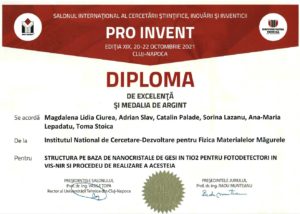
- Diploma of Excellence and Silver Medal (“Diploma de Excelenta si Medalia de Argint”) for “Structure based on GeSi nanocrystals embedded in TiO2 for VIS-NIR photodetectors and fabrication method” (“Structura pe baza de nanocristale de GeSi in TiO2 pentru fotodetectori in VIS-NIR si procedeu de realizare a acesteia”) awarded to M.L. Ciurea, A. Slav, C. Palade, S. Lazanu, A.M. Lepadatu at ProInvent (International Exhibition of Research, Innovations and Inventions), XIXth ed., Cluj-Napoca 2021
- Success Story in 2018 for M-Era.Net Project "High photoconductive oxide films functionalized with GeSi nanoparticles for environmental applications” (https://m-era.net/success-stories/high-photoconductive-oxide-films-functionalized-with-gesi-nanoparticles-for-environmental-applications-photonanop; https://m-era.net/news/success-stories-booklet-2-has-been-published)
- CAS 2018 BEST PAPER AWARD for “GeSi nanocrystals in SiO2 matrix with extended photoresponse in near infrared”, I. Stavarache, L. Nedelcu, V.S. Teodorescu, V.A. Maraloiu, I. Dascalescu, M.L. Ciurea
Research stages
- Working visit of PhD student Muhammad Taha Sultan (RU-SSE) at NIMP, between 23th June and 11th July: preparation of test samples; electrical and photoelectrical measurements on NIMP and RU-SSE test samples within PhotoNanoP research project
PROJECTS/ INTERNATIONAL PROJECTS
Copyright © 2024 National Institute of Materials Physics. All Rights Reserved