Broadband photodetector based on hydrogenated GeSn layers
Project Director: Dr. Adrian SLAV
Stage I and II /2021
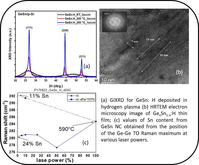
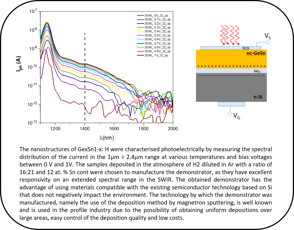
Photoconductive GexSn1-x:H nanostructures with various Sn concentrations in GeSn nanocrystals were obtained by the magnetron sputtering method . The hydrogenation of the structures was done by RTA in the temperature range 150 oC – 400 oC in the atmosphere of H2 and by deposition in working gas (Ar) with 10% and 30% H. In the case of in-situ hydrogenation the substrate temperature was maintained at 30 oC (RT) and 200 oC. For GexSn1-x co-deposited and hydrogenated by RTA, through increasing the annealing temperature and the Sn concentration we obtained the increasing of the Ge:Sn ratio in the GeSn nanocrystals, simultaneously with the increase the content of segregated Sn in the β-Sn phase. GeSn nanocrystals are formed at low annealing temperatures (150 oC and 300 oC) without arising the β-Sn phase (up to 400 oC). By increasing the annealing temperature, the Sn concentration in nanocrystals decrease down to ~ 7%. Shifting diffraction peaks to small 2q angle shows that the lattice constant increase by including Sn in the Ge crystalline lattice. Electron microscopy images shows columnar crystalline areas alternating with amorphous zones with lengths of 25 – 35 nm and 7 nm size. By EDX compositional analysis the Sn concentrations was evaluated between 7.55% and 9.94%, values that are in good agreement with the results obtained by µ-Raman spectroscopy. Also, from XPS we found similar values for Sn concentration in the GeSn nanocrystals. From the Tauc representation of the optical absorption coefficient we evaluate the effect of hydrogenation on defect states. Also, by FT-IR spectroscopy the Ge-H vibration mode was evidenced at 1873 cm -1. The I-V electrical measurements showed a strong rectifying character of the GexSn1-x:H structures at low temperatures due to the GeSn heterojunction with the Si support. For the GexSn1-x:H samples with 30% H, the spectral response was extended up to 2 µm in comparison to samples with weaker hydrogenation (10%). In addition, better hydrogenation decreases the dependence of the photocurrent on the bias voltage by reducing the defect states in the gap.
Stage III /2022
- "Nanocrystallized Ge-rich SiGe-HfO2 Highly Photosensitive in Short-Wave Infrared", C. Palade, A.M. Lepadatu, A. Slav, V.S. Teodorescu,T. Stoica, M.L. Ciurea, D. Ursutiu, C. Samoila , Materials 2021, 14, 7040;
https://doi.org/10.3390/ma14227040 - „From Si nanowires to Ge nanocrystals for VIS-NIR-SWIR sensors and non-volatile memories: A review”, A.M. Lepadatu, I. Stavarache, C. Palade, A. Slav, V.A. Maraloiu, I. Dascalescu, O. Cojocaru, V.S. Teodorescu, T. Stoica, M.L. Ciurea, Annals of the Academy of Romanian Scientists Series on Physics and Chemistry Sciences 7(1), 53-87 (2022);
- „Extended near infrared photo-response influenced by host matrix change in Ge nanoparticle-based films”, IEEE International Semiconductor Conference (CAS) 45th edition CAS 2022, Poiana Brasov, 12-14 octombrie, IEEE CAS 2022 Proceedings, pp. 231-234
- “Memory properties of Zr doped ZrO2 MOS-like capacitor”, Palade, A. Slav, I. Stavarache, V.A. Maraloiu, C. Negrila, M.L. Ciurea, Coatings 12, 1369 (2022)
- “From GeSi to SiGeSn alloy nanocrystals with benefits in SWIR detection”, M.L. Ciurea, T. Stoica, I. Stavarache, A.-M. Lepadatu, C. Palade, A. Slav, I. Dascalescu, O. Cojocaru, 13th International Conference on Physics of Advanced Materials (ICPAM-13), 24-30 sep. 2021, Sant Feliu de Guixols, Costa Brava, Spain, oral presentation, https://icpam.ro/invited-speakers/
- “Synergistic enhancement of SWIR photosensitivity in nanocrystals/epitaxial heterojunctions of GeSn layers”, Dascalescu, N.C. Zoita, A. Slav, A.‐M. Lepadatu, C. Palade, D. Buca, V.S. Teodorescu, M.L. Ciurea, M. Braic, T. Stoica, EMRS 2021 Fall Meeting, 20-23 septembrie 2021, oral presentation;
- “Nanocrystallization of GeSn thin layers controlled by SiO2 spacer in multilayers”, Slav, I. Dascalescu, A.-M. Lepadatu, C. Palade, V.S. Teodorescu, M.L. Ciurea, M. Braic, T. Stoica, 2021 International Semiconductor Conference, 6 – 8 October 2021, oral presentation;
- „GexSn1-x:H thin film with high spectral response in SWIR range deposited by magnetron sputtering”, A. Slav, C. Palade, I. Stavarache, G.A. Lungu, M.Braic, S. Iftimie, V.S. Teodorescu, M.L. Ciurea, T. Stoica, 14th International Conference on Physics of Advanced Materials (ICPAM-14), Dubrovnik, Croatia, 8 – 15 September, 2022 – oral presentation;
- „Strained Ge-rich SiGe nanocrystals in nanocrystallized HfO2 layers for extended VIS-SWIR photoelectric sensitivity”, A. M. Lepadatu, C. Palade, A. Slav, V. S. Teodorescu, T. Stoica, M. L. Ciurea, 2022 Spring Meeting of the European Materials Research Society (E-MRS), VIRTUAL Conference, May 30 – June 3, 2022 – oral presentation;
- „SiGe nanocrystals in TiO2 with extended SWIR photosensitivity for photonics", O. Cojocaru, C. Palade, A. Slav, A.M. Lepadatu, V.S. Teodorescu, T. Stoica, M.L. Ciurea, Conferinta Stiintifica de Primavara a AOSR, 2022, Bucuresti – oral presentation;
- „Extended near infrared photo-response influenced by host matrix change in Ge nanoparticle-based films”, I. Stavarache, C. Palade, A. Slav, P. Prepelita, V.S. Teodorescu, M.L. Ciurea, IEEE International Semiconductor Conference (CAS) 45th edition CAS 2022, October 12 -14, 2022, Poiana Brasov, Romania – Premiu „Best Paper Award”.
Patents:
- OSIM patent application no. A/00646 of October 18, 2022 "Procedure for obtaining a thin film of passivated GeSn, with increased photosensitivity in SWIR", A. Slav, T. Stoica, I.-M. Dascalescu, C. Palade, G.-A. Long.
PROJECTS/ NATIONAL PROJECTS
Copyright © 2026 National Institute of Materials Physics. All Rights Reserved