Project Cod: , PN-III-P2-2.1-PED-2021-3165
Project Director : Dr. Anca Stanculescu
Project type: National
Program: Program 2: P2 - Increasing the competitiveness of the Romanian economy through CDI; Subprogram Competitiveness through research, development and innovation (partially); Experimental Demonstration Project (PED)
Founded by: The Executive Agency for Higher Education, Research, Development and Innovation Funding(UEFISCDI)
Contractor: National Institute of Materials Physics
Status: In development
Start date: 30.06.2022
End date: 30.06.2024
Summary
The organic phototransistors (OPTs) are optical transducer based on organic field effect transistors (OFETs) showing good absorption in a specific domain and high efficiency of photocurrent generation, with many applications in industrial, military, environmental and biological sectors.
The project is focused on obtaining OFET structures on flexible substrate with improved properties, sensitive to UV-VIS illumination, avoiding the use of expensive and limited resources raw materials (indium).
In the frame of this project will be developed original ideas concerning: the active layer for OFET from oligomers/polymers based on arylaminic derivatives; transistor channel type bulk heterojunction (BHJ), mixed layer from the mentioned donors and a non-fullerene perylene diimide derivative acceptor; transparent gate electrode indium-free made from Al doped ZnO ; modification of the surfaces/interfaces by nanostructuring.
For an increase from TRL 2 (concept of OFET sensible to UV-VIS radiation) to TRL 3 (experimental demonstrator of a flexible, ambipolar OFET with reproducible electrical parameters in dark and response under illumination) are proposed the following objectives: 1. Preparation of active layer from new organic compounds and transparent gate electrode for OFET structures. 2. Realization of new nanostructured OFET structures sensible to UV-VIS radiation
The project feasibility is sustained by the preliminary experimental results and expertise concerning the synthesis of the compounds (PPIMC/P1), transparent conductor electrodes (INFLPR/P2), organic thin film (CO+P2) and nanostructuring (CO), research strategy and infrastructure of the partners. CO will be in charge with the realization of the OFETs and their characterization in dark and at illumination, P1 with the synythesis, purification and characterization of the compounds for channel material and P2 with the deposition of transparent conductor electrode and of the mixed layer (BHJ).
National Institute of Materials Physics (NIMP) -CO
Dr. Anca Stanculescu-Project Director
Dr. Nicoleta Preda-scientific researcher 1
Dr. Marcela Socol-Scientific researcher 1
Dr. Oana Rasoga-Scientific researcher 2
Dr. Carmen Breazu-Scientific researcher 3
Dr. Paul Ganea-scientific researcher 3
Gabriela Petre -PhD student
"P. Poni" Institute of Macromolecular Chemistry (PPIMC)-P1
Dr. Andrei Honciuc-Partner Responsible
Dr. Ana-Maria Solonaru-Scientific researcher
Dr. Oana-Iulia Negru-Research assistant
National Institute for Laser, Plasma and Radiation physics (NILPRP)-P2
Dr. Gabriel Socol- Partner Responsible
Dr. Gianina Popescu-Pelin-Scientific researcher 3
Andreea Mihailescu-Research assistant, PhD student
Andrei Stochioiu-PhD student
Ion Tudor-technician
Stage 1: Preparation of channel active layer from new organic compounds and transparent gate electrode for OFET structures
In the frame of this stage we have synthetized and preliminary characterized organic compounds (donors and acceptors) which will be utilized in the next stages for the preparation of the channel active material in organic field effect transistor (OFET) structure. Perylene diimides have been proposed as acceptors because of their high electrons affinity, high light absorption coefficient and good transport properties. By functionalization, in different positions, with alkyl or aryl group to the nitrogen atoms, the solubility in common solvents is improved, the segregation is prevented and the preparation of high quality thin films adequate for electronic applications (OFETs), is favored. Good absorption in visible domain and a position of the HOMO and LUMO levels favoring the charge transport which is not trap-limited, have been revealed for the selected acceptor compound that contains the alkyl substituent group. Two arylenvinylene based monomers and intermediary monomers for the preparation of polymers with arylenvinylene and arylenethynilene structure containing 2,7-dibrom N-(2-ethyl-hexyl) were also synthetized. These compounds, showing extended absorption and good transport of the carriers, will be used as donors.
Transparent conducting oxide/TCO layers (Al:ZnO/AZO; In:ZnO/IZO90) were deposited by PLD on different flexible substrates: PES 0.25 mm, PES 0.5 mm, PET amorphous; PET biaxial oriented and flexible glass. Correlating the morphological properties (uniform deposition) with those of transmission (>90 %) and sheet resistance (~5x10² ohm/□), the PES 0.5 mm and PES 0.25 mm substrates can be selected for the deposition of the AZO and IZO90 transparent conductor layer.
Uni-component (donor, acceptor) and mixed donor (arylenvinylene monomer):acceptor (perylene diimide derivative) layers were prepared on the mentioned substrates using the vacuum evaporation and deposition technique. FTIR analysis has confirmed the deposition of mixed layers containing the both components and the preservation of the chemical structure of the donor and acceptor, during the deposition process. The optical analysis has revealed that, in principle, all types of substrate can be utilized for the deposition of the organic films which show absorption bands both in UV and Vis, with the exception of PES 0.25 mm which cut the signal for wavelengths <400 nm. Considering the losses by radiative relaxation mechanisms, PET amorphous, PET biaxially oriented and flexible glass have resulted as the most appropriate substrates for the deposition of simple and mixed organic layers from the selected compounds for Vis applications and flexible glass for UV applications. Correlating the transmission and photoluminescence results, the PES 0,25 mm substrate can not be used in UV domain. Taking into account, both the morphology of the layer (low roughness can reduce the scattering) and the optical properties, flexible glass is a good option of substrate for the deposition of mixed organic layers. The dielectric properties of the organic layer are not significantly affected by the type of substrate and thus they don’t have a critical role in the selection of the substrate. Considering the electrical properties of the TCO and organic layer, PES 0.5 mm and PES 0.25 mm are the most appropriate substrates for deposition. Therefore, choosing the substrate for the realization of the heterostructure it is a process that requires the consideration of several factors such as: type and properties of the TCO layer, composition and properties of the mixed layer. The substrate covered by the transparent conductor (the gate in OFET structure) must be transparent in UV and/or Vis and the organic layer must absorb the UV and/or Vis radiation that will be involved in the generation of charge carriers.
In conclusion, the objectives of this stage have been achieved: donors and acceptor compounds have been synthetized and characterized, transparent conductor layers and organic layers have been deposited on flexible substrates. The layers were characterized from morphologic, optic, electric, dielectric point of view, in order to be selected in correlation with the type of substrate. The heterostructure with mixed organic layer (monomer based on arylenvinylene):acceptor (perylendiimide) deposited on flexible AZO showed the best transport properties.
Stage 2: Realization of new nanostructured OFET structures with reproducible parameters
During this stage were investigated organic compounds from the azomethine group containing carbazole or triphenylamine groups, two polymers with an arylenevinylene structure based on 2,7 carbazole (H) or 3,6 carbazole and the monomer 2,7-dibromo-N-2-ethyl-hexyl carbazole (MH) as donors and a non-fullerene compound, derivative of perylenediimide, studied in comparison with a fullerene derivative, as acceptor in the mixed layers for the channel of an organic field effect transistor (OFET) structure on a rigid/flexible, flat/nano-patterned substrate. Poly(arylenevinylenes) are photoluminescent conductive polymers due to the presence of single and multiple alternative bonds, but they present insolubility and infusibility that make them difficult to process. This disadvantage can be removed by intercalating N-alkyl carbazole units in the polymer structure because carbazole, like oligomers and polymers based on this monomer, have good optical and electronic properties, electrochemical reversibility, high charge carrier mobility and structural stability. Perylene tetracarboxyl diimide (PDI) is used as an acceptor because its improved solubility, through functionalization with the alkyl group at the nitrogen atoms, prevents aggregation, it has good absorption in the visible and a position of the HOMO and LUMO levels favorable for carrier transport that is not limited by the phenomenon of " trapping". These mixed layers were characterized optically, morphologically and electrically, and those presenting a good UV-Vis absorption, a good transport of the charge carriers and the lowest roughness, in order to avoid losses through the scattering or recombination of the charge carriers, were selected : 1) the monomer (MH) as donor and PDI as acceptor for the bi-layer OFET structure, on a flexible nanostructured substrate; 2) polymer (H) as donor and PDI as acceptor to realize the bulk heterojunction active material (BHJ) for the channel of the OFET structure. To make the OFET, the layers of the structure were deposited in a well-defined sequence -the gate electrode, gate insulator, active layer, source-drain electrodes, using special masks (Ossila for OFET-low density) and a self-made mask adaptor for vaccum evaporation equipment. To obtain the nanostructured transparent conductive electrode (AZO, IZO70, IZO90), the UV NanoImprint Lithography method was used, generating a 2D network of nanostructures with the following geometric parameters: cylinders with a diameter of 400 nm, periodicity of 1.1, mm and height of ~300 nm. Because the nanostructuring of a layer deposited on a flexible substrate is very difficult and because PES is the substrate that has thermal and mechanical properties that allows the processes involved in nanostructuring to be carried out, without damage, it was chosen to create flexible nanostructured OFET structures on PES. The studies for the selection of the gate insulator involved the comparative analysis of the optical-morphological and dielectric properties of three materials: poly(methyl methacrylate) and 2 nucleic acid bases, cytosine and guanine, and led to the selection of cytosine as organic material for the gate insulator.
Active bi-layer OFET structures on flat and nanopatterned substrate were prepared and investigated: PETamorph/ITOflat/cytosine/MH/PDI/Al compared to glass/IZO70flat/cytosine/MH/PDI/Al and PES0.25 nanostructured/IZO70; IZO90; AZO/cytosine/MH/PDI/Al. Also, in advance were done the first experiments to create the OFET structure on a flexible substrate with mixed layer: PES0.25; PES0,5; PET amorph/IZO70; IZO90; AZO/cytosine/H:PDI in weight ratio (1:2)/Al. For these structures, the curves gate current=f(source-gate voltage) and drain current=f(source-drain voltage) were drawn. The selected OFET bi-layer structure with a channel of two overlapping organic layers, on a nanostructured flexible substrate is PESnano/IZO90/cytosine/MH/PDI/Al, that shows small drain currents when varying the source-drain voltag, that increase by two orders of magnitude upon illumination. The electrical properties of the gate insulating layer are essential for improving the properties of the OFET structures. The preliminary results indicate for the OFET structure with a bulk heterojunction channel (BHJ), on a flexible substrate, PES0.5/IZO70/cytosine/H:PDI (1:2)/Al, show FET characteristics drain current=f(source-drain voltage) in the dark, with an estimated threshold voltage of ~1 V.
In conclusion, the objectives and estimated results of the stage 2 were achieved: organic compounds were synthesized, characterized and selected as donor and acceptor for the mixed layers that can be used in the realization of the bulk heterojunction (BHJ) type channel for flexible OFET. The synthesis processes have been improved with an effect on the purity and properties of the compounds. The nanostructured flexible electrode was obtained and the flexible nanostructured OFET structure with an active layer of two overlapping layers (bi-layer) was built on it. The bi-layer OFET structures were characterized and the structure that presents the best electrical behavior (PESnano/IZO90/cytosine/MH /PDI/Al) was selected.
Stage 3: Studies on the response of the OFET structures under UV-Vis illumination
During this stage were investigated some compounds as active material for the channel of an organic field effect transistor (OFET) structure: organic polymeric arylamide compounds containing the substituted carbazole group in the positions 2,7 [poly(N-(2-ethylhexyl-2,7 carbazolyl)vinylene-H2] and 3,6 [poly(N-(2 -ethylhexyl-3,6 carbazolyl)vinylene-H3] as donors, and a fullerene derivative compound as acceptor in mixed layers and, the oligomer 2,7dibromo-N-2-(ethylhexyl)carbazole] (MH) as donor and a non-fullerene compound, derivative of perylenediimide N,N'-bis(dodecyl) - 3, 4, 9, 10-tetracarboxyl perylenediimide (AMC14) as acceptor in bi-layer sandwich structures. Flexible substrates, plane and nanostructured, as well as rigid substrate (glass), were covered with conductive transparent layers of AZO, IZO70, IZO90, ITO as gate and layers of bio materials such as the nitrogenous bases of nucleic acids (guanine, cytosine, adenine) as insulator of the gate. Carbazole-based polymers were selected because carbazole-based oligomers and polymers have good optical and electronic properties. As acceptor, were selected a compound from the perylene family and a high rank analog of fullerene, [6,6]-phenyl C71 butyric acid methyl ester, [70]PCBM, characterized by an increased absorption in the visible region of the spectrum because the energy transitions that are forbidden in C60 are allowed by the non-symmetrical "cage" of C70 in [70]PCBM, by a high mobility of the charge carrier and by an increased solubility in common solvents. The mixed layers were analyzed from the point of view of optical, morphological and electrical properties. It was highlighted that the mixed layers containing the polymer with the shorter conjugation length, with substitutions in the 3,6 positions presented a better conductance than those containing the polymer with the longer conjugation length, with substitutions in the 2,7 positions, for weight ratio donor:acceptor (1:1) and (1:3), behavior affected by the morphology of the mixed layer.
The choice of the substrate must take into account many factors (losses through radiative relaxation mechanisms, morphology, compatibility with the nano-patterning process) being a compromise between them. Following the investigations, PES was selected for the nanostructuring by UV Nano-Imprint Lithography, in order to obtain the nanostructured gate electrode. The I-V characteristics were plotted for 9 different types of OFET structures on flexible (PET, PES) and rigid substrate, with different gate electrodes (AZO, IZO70 and IZO90) planar and nanostructured with different organic gate insulators and channel material mixed (arylenvinylene polymers: perylene derivative) and bi-layer (monomers:perylene derivative).
The output characteristics for the sample made with a mixed layer polymer:perylenediimide derivative in weight ratio of 1:2 and with a gate insulator from a nucleic acid base highlighted the ambipolar conduction of the channel: p-type channel (holes accumulated inside the channel) in quadrant 3 and an n-type channel (electrons accumulated inside the channel) in quadrant 1. OFET structures were illuminated with Vis radiation in pulsed mode with a symmetrical rectangular signal and the response (drain current) was drawn as a function of time, in transient mode of operation, revealing a sudden increase in current when the signal was applied. The most significant increase in current (~ 2 orders of magnitude) in response at pulsed Vis illumination was obtained by the OFET made with a mixed layer on a planar flexible substrate PES0.5/IZO70/cytosine/H2:AMC14 (1:2)/Al. The most important response in current at continuous UV illumination was obtained by the OFET made on nanostructured PES with the monomer (MH) and perylene derivative (AMC14). The increase in the current during continuous illumination compared to the current in the dark was ~ 2 orders of magnitude, for a gate voltage UG=0. Both in Vis and UV lighting, the characteristic drain current depending on drain voltage shows hysteresis.
In conclusion, the objectives and estimated results of the 2024 phase were achieved and all the activities proposed to each partner were carried out: OFET structures were made by CO and P2 on a nanostructured and planar substrate with the mixed-layer and bi-layer channel material from the compounds synthesized by P1. These structures were characterized in dark and their response to UV and Vis illumination was comparatively investigated. The structures that gave the best response to Vis illumination, in the transient regime, were PESnano/IZO70/adenine/H3:AMC14 (1:2)/Al, PES0.5/IZO70/cytosine/H2:AMC14 (1 :2)/Al and PESnano/AZO/cytosine/MH/AMC14/Al. The OFET structure PESnano/AZO/cytosine/MH/AMC14/Al presented the best response to continuous UV illumination.
Brief presentation of the project results
Organic phototransistors are optical transducers based on organic field-effect transistors (OFETs) characterized by good absorption in a specific spectral domain and high efficiency in photocurrent generation, having many industrial, military, environmental and biological applications.
The goal of the project is to obtain OFET structures on a flexible substrate, sensitive to UV-VIS illumination, avoiding the use of expensive materials and technologies, such as those involved in the realization of conventional, inorganic field-effect transistors.
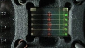 | 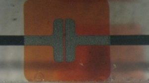 |
| Flexible substrate with 5 OFET structures mounted in the board for OFET characterization. | Detail of one OFET structure showing the active layer and, source and drain electrodes. |
The original ideas developed in this project refer to: 1) the active layers for the channel of the field-effect transistor as bulk heterojunction (BHJ), mixed layer formed by arylaminic polymers [poly(N-(2-ethylhexyl-2,7 carbazolyl)vinylene-H2 ; poly(N-(2-ethylhexyl-3,6 carbazolyl)vinylene-H3 ] and non-fullerene acceptors from perylenediimide derivatives [N, N'-bis(dodecyl)- 3, 4, 9, 10- tetracarboxyl perylendiimide-AMC14]; 2) gate electrode from a transparent conductor, ZnO doped either with Al (AZO) or In (IZO70, IZO90); 3) gate insulator from a bio material, a base of nucleic acids (cytosine) and 5) modification of surfaces/interfaces by nanostructuring using UV-NanoImprint Lithography. These ideas were integrated and used in the realization of organic field effect transistor structures.
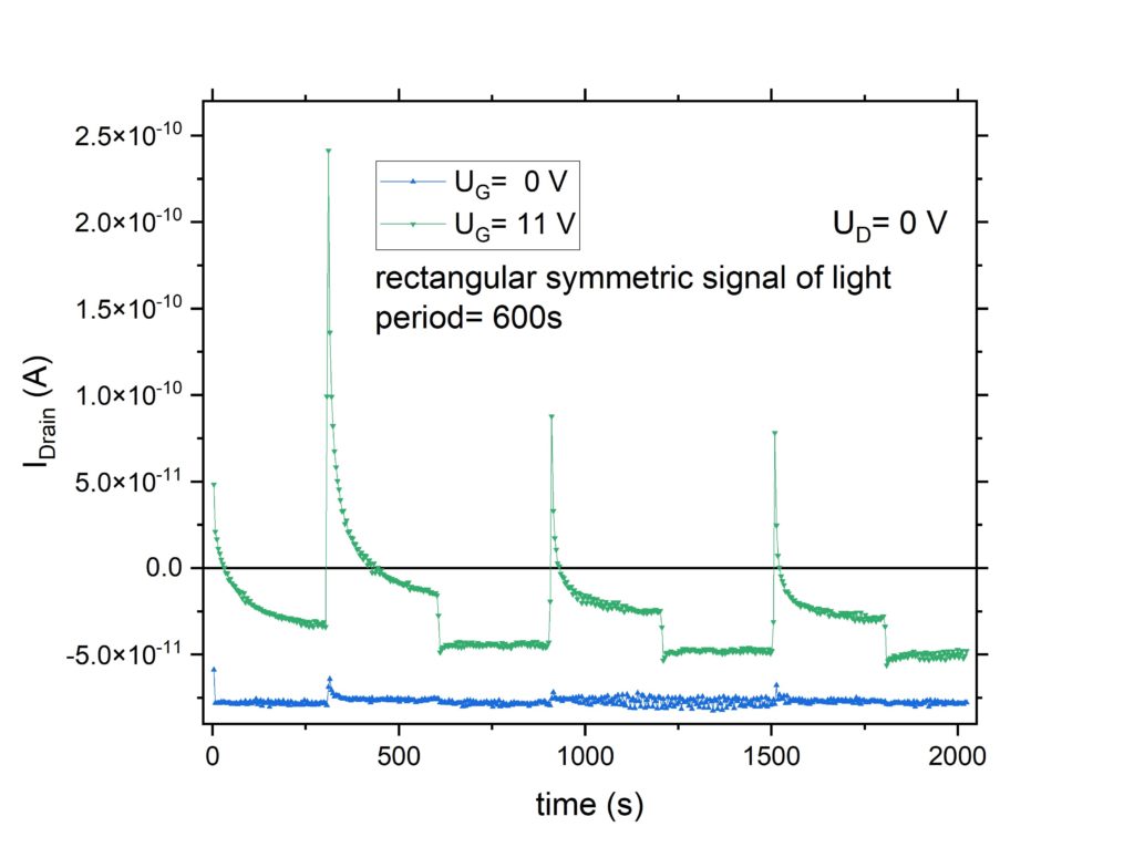 |  |
| The variation of the drain current as a function of time for the structure PES0,5/IZO70 /citozina/H2:AMC14 (1:2)/Al.
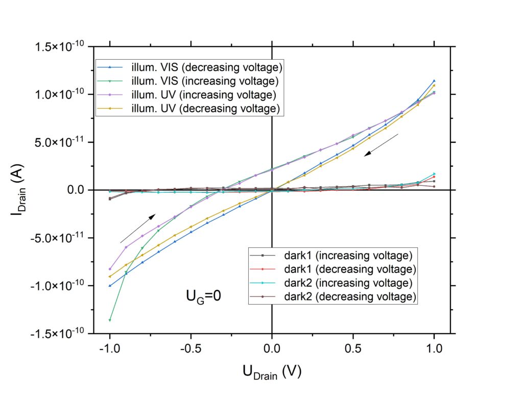
| The variation of the drain current as a function of the drain voltage under UV and continuous Vis illumination for the structure: PESnano/AZO/citozina/ MH/AMC14/Al.
|
The most significant increase in response current to Vis illumination in pulses was obtained for the OFET structure made with a mixed layer on a planar flexible substrate PES0.5/IZO70/cytosine/H2:AMC14 (1:2)/Al, and for continuous illumination in the UV domain was obtained by the OFET structure made on nanostructured PES with the monomer [2,7dibromo-N-2-(ethylhexyl) carbazole [MH] and N, N'-bis(dodecyl)- 3, 4, 9, 10- tetracarboxyl perylenediimide [AMC14]. The current increased with ~ 2 orders of magnitude during illumination compared to dark, for a gate voltage UG=0.
Stage 1 (2022)
1 paper communicated at: “7th European Congress on Advanced Nanotechnology and Nanomaterials Webinar” November 14th- 15th, 2022, Rome, Italy.
Title: "Organic heterostructure with dendrimer:non-fullerene mixed layer for electronic applications"
Authors: C. Breazu1, A. Lutgarde Djoumessi Yonkeu2, O. Rasoga1, M. Socol1, N. Preda1, G. Petre1,3,F. Stanculescu3, A. Stanculescu1, E. Iwouha2
1National Institute of Materials Physics, Atomistilor 405A, 077125, Magurele, Romania, 2University of Western Cape, Department of Chemistry, SensoLab, Robert Sobukwe Road, P. Bag X17, Bellville 7535, Cape Town, South Africa3, University of Bucharest, Faculty of Physics, 405 Atomistilor Street, P.O. Box MG-11, Bucharest-Magurele, 077125 Romania, 4Laboratoire LPHIA, Université d’Angers, LUNAM 2, Bd. Lavoisier 49045, Angers, France
1 paper accepted for publication in Nanomaterials
Title: Effect of Aluminum nanostructured electrode on the properties of bulk heterojunctions based heterostructures for electronics, Nanomaterials, 12, 4230 (2022)
Authors: Oana Rasoga1, Carmen Breazu1, Marcela Socol1, Ana-Maria Solonaru2, Loredana Vacareanu2, Gabriela Petre1,3, Nicoleta Preda1, Florin Stanculescu3, Gabriel Socol4, Mihaela Girtan5, Anca Stanculescu1
1National Institute of Materials Physics, 405A Atomistilor Street, P.O. Box MG-7Magurele, 077125 Romania; 2P. Poni Institute of Macromolecular Chemistry, 41 A Gr. Ghica Voda Alley, 700487, Iasi, Romania; 3University of Bucharest, Faculty of Physics, 405 Atomistilor Street, P.O. Box MG-11, Magurele, 077125 Romania; 44National Institute for Laser, Plasma and Radiation Physics, Str. Atomistilor, Nr. 409, PO Box MG-36, Bucharest, 077125, Romania; 5Laboratoire LPHIA, Université d’Angers, LUNAM, 2 Bd. Lavoisier 49045, Angers, France
Stage 2 (2023)
Paper published in Thin Solid Films:
Title: Organic heterostructures based on thermal evaporated phthalocyanine and porphyrin as mixed (ZnPc:TpyP) or stacked (ZnPc/TpyP) films, Thin Solid Films, 87, 140140 (2023)
Authors: G. Petre1,2, M. Socol1,N. Preda1, C. Breazu1, O. Rasoga1, F. Stanculescu2, A. Costas1, S. Antohe2, S. Iftimie2, G. Socol3, A. Stanculescu1;
1 National Institute of Materials Physics, 405 bis Atomistilor Street, P.O. Box MG-7, Bucharest-Magurele, 077125 Romania; 2University of Bucharest, Faculty of Physics, 405 Atomistilor Street, P.O. Box MG-11, Bucharest-Magurele, 077125 Romania; 3National Institute for Laser, Plasma and Radiation Physics, Str. Atomistilor, Nr. 409, PO Box MG-36, Magurele, Bucharest, 077125, Romania
Papers sent for publication
1) Title: Perylene diimide derivative based binary and ternary layers obtained by a laser technique for optoelectronic applications; sent to Optics and Laser Technology, manuscript number: JOLT-D-23-02301 (under review).
Autori: C. Breazu1, A. Stanculescu1, O. Rasoga1, N. Preda1, A. Costas1, A. M. Catargiu2, G. Socol3, G. Popescu-Pelin2, A. Stochioiu2, S. Iftimie4, G. Petre1,4, M. Socol1
1 National Institute of Materials Physics, 405 bis Atomistilor Street, P.O. Box MG-7, Bucharest-Magurele, 077125 Romania; 2P. Poni Institute of Macromolecular Chemistry, 41 A Gr. Ghica Voda Alley, 700487-Iasi, Romania;3National Institute for Laser, Plasma and Radiation Physics, Str. Atomistilor, Nr. 409, PO Box MG-36, Magurele, Bucharest, 077125, Romania; 4University of Bucharest, Faculty of Physics, 405 Atomistilor Street, P.O. Box MG-11, Bucharest-Magurele, 077125 Romania
2)Titlu: Organic heterostructures with dendrimer based mixed layer for electronic applications; sent to Molecules, manuscript ID: molecules-2772476 (under review)
Autori: O. Rasoga, A. Djoumessi Yonkeu, C. Breazu, M. Socol, N. Preda, F. Stanculescu, A. Stanculescu, E. Iwuoha
1National Institute of Materials Physics, Atomistilor 405A, 077125, Magurele, Romania; 2University of Western Cape, Department of Chemistry, SensoLab, Robert Sobukwe Road, P. Bag X17, Bellville 7535, Cape Town, South Africa; 3University of Bucharest, Faculty of Physics, 405 Atomistilor Street, P.O. Box MG-11, Bucharest-Magurele, 077125 Romania
Papers presented at conferences
1) EMRS Spring Meeting 2023, Symposion L: Making light matter: lasers in material sciences and photonics, 29 May-2 June, Strasbourg, France-poster.
Title: Organic heterostructures with nanopatterned electrode and nanoparticle buffer layer prepared by laser technique;
Authors: C. Breazu1, M. Socol1, O. Rasoga1, G. Petre1,5, N. Preda1, I. Zgura1, A. Honciuc2, A. M. Solonaru2, G. Socol3, G. Popescu-Pelin3, M. Girtan4, F. Stanculescu5, C. Thanner6, A. Stanculescu1;
1 National Institute of Materials Physics, 405 bis Atomistilor Street, P.O. Box MG-7, Bucharest-Magurele, 077125 Romania; 2P. Poni Institute of Macromolecular Chemistry, 41 A Gr. Ghica Voda Alley, 700487-Iasi, Romania;3National Institute for Laser, Plasma and Radiation Physics, Str. Atomistilor, Nr. 409, PO Box MG-36, Magurele, Bucharest, 077125, Romania; 4University of Angers, Photonics Laboratory, University 2, Bd. Lavoisier 49045, Angers, France; 5University of Bucharest, Faculty of Physics, 405 Atomistilor Street, P.O. Box MG-11, Bucharest-Magurele, 077125 Romania; 6EVGroup., DI Erich Thallner Strasse 1, 4782 St. Florian am Inn, Austria .
2) EMRS Spring Meeting 2023, Simpozion Q: Advanced functional films grown by pulsed deposition methods, 29 May-2 June, Strasbourg, France-poster.
Title: Effect of laser deposited flexible transparent conductor electrode on the properties of organic heterostructures;
Authors: G. Petre1, G. Socol2, M. Socol1, C. Breazu1, O. Rasoga1, N. Preda1, P. Ganea1, A. Honciuc3, A. M. Solonaru3, O. I. Negru3, G. Popescu-Pelin2, A. Mihailescu2, A. Stochioiu2, F. Stanculescu4, A. Stanculescu1;
1 National Institute of Materials Physics, 405 bis Atomistilor Street, P.O. Box MG-7, Bucharest-Magurele, 077125 Romania; 2National Institute for Laser, Plasma and Radiation Physics, Str. Atomistilor, Nr. 409, PO Box MG-36, Magurele, Bucharest, 077125, Romania; 3P. Poni Institute of Macromolecular Chemistry, 41 A Gr. Ghica Voda Alley, 700487-Iasi, Romania; 4University of Bucharest, Faculty of Physics, 405 Atomistilor Street, P.O. Box MG-11, Bucharest-Magurele, 077125 Romania.
3)The 15th International Conference on Physics of Advanced Materials (ICPAM 15), Topic T1: Thin Films and Nanostructures for Modern Electronics, 19-26 November 2023, Sharm El Sheikh, Egypt-invited paper.
Title: Effect of nanostructuring on the properties of organic heterostructures with single stacked bi and mixed layer;
Authors: A. Stanculescu1, C. Breazu1, O. Rasoga1, G. Socol2, G. Popescu-Pelin2, G. Petre1,3, M. Socol1, F. Stanculescu3;
1 National Institute of Materials Physics, 405 bis Atomistilor Street, P.O. Box MG-7, Bucharest-Magurele, 077125 Romania; 2National Institute for Laser, Plasma and Radiation Physics, Str. Atomistilor, Nr. 409, PO Box MG-36, Magurele, Bucharest, 077125, Romania; 3University of Bucharest, Faculty of Physics, 405 Atomistilor Street, P.O. Box MG-11, Bucharest-Magurele, 077125 Romania
Stage 3 (2024)
Papers sent for publication
1) Title: Organic heterostructures with dendrimer based mixed layer for electronic applications; sent to Molecules, (sent revision)
Authors: O. Rasoga, A. Djoumessi Yonkeu, C. Breazu, M. Socol, N. Preda, F. Stanculescu, A. Stanculescu, E. Iwuoha
1National Institute of Materials Physics, Atomistilor 405A, 077125, Magurele, Romania; 2University of Western Cape, Department of Chemistry, SensoLab, Robert Sobukwe Road, P. Bag X17, Bellville 7535, Cape Town, South Africa; 3University of Bucharest, Faculty of Physics, 405 Atomistilor Street, P.O. Box MG-11, Bucharest-Magurele, 077125 Romania
2) Title: Flexible azomethine-perylenediimide bulk heterojonction deposited by MAPLE for optoelectronics; sent to Synthetic Metals
Authors: C. Breazu1, M. Socol1, G. Petre1, G. Socol2, G. Popescu-Pelin2, N. Preda1, A. –M. Solonaru3, M. Girtan4, F. Stanculescu5, A. Stanculescu1, O. Rasoga1
1National Institute of Materials Physics, Atomistilor 405A, 077125, Magurele, Romania;2 National Institute for Laser, Plasma and Radiation Physics, Str. Atomistilor, Nr. 409, PO Box MG-36, Magurele, Bucharest, 077125, Romania;3P. Poni Institute of Macromolecular Chemistry, 41 A Gr. Ghica Voda Alley, 700487-Iasi, Romania; 4University of Angers, Photonics Laboratory, University 2, Bd. Lavoisier 49045, Angers, France; 5University of Bucharest, Faculty of Physics, 405 Atomistilor Street, P.O. Box MG-11, Bucharest-Magurele, 077125 Romania
3)Title: MAPLE deposited perylene diimide derivative based layers for optoelectronic applications; sent Journal of Materials Science
Authors: C. Breazu1, M. Girtan2, A. Stanculescu1*, N. Preda1, O. Rasoga1, A. Costas1, A. M. Solonaru3, G. Socol4, G. Popescu-Pelin4, A. Stochioiu4,5, S. Iftimie5, G. Petre1,5, M. Socol1
1National Institute of Materials Physics, Atomistilor 405A, 077125, Magurele, Romania; 2University of Angers, Photonics Laboratory, University 2, Bd. Lavoisier 49045, Angers, France;3P. Poni Institute of Macromolecular Chemistry, 41 A Gr. Ghica Voda Alley, 700487-Iasi, Romania; 4National Institute for Laser, Plasma and Radiation Physics, Str. Atomistilor, Nr. 409, PO Box MG-36, Magurele, Bucharest, 077125, Romania; 5University of Bucharest, Faculty of Physics, 405 Atomistilor Street, P.O. Box MG-11, Bucharest-Magurele, 077125 Romania
Papers presented at conferences
EMRS Spring Meeting 2024, Sympozion V: 6th EMRS &MRS-K bilateral symposium "X-tronics: optoelectronic and bioelectronic-from materials to devices",27 mai-31 mai, Strasbourg, Franta-poster
Title: Flexible nanostructured bio-organic field effect transistor;
Authors: A. Stanculescu1, C. Breazu1, M. Socol1, O. Rasoga1, G. Petre1,4, N. Preda1, P. Ganea1, A. Honciuc2, A. M. Solonaru2, O. I. Negru2, G. Socol3, G. Popescu-Pelin3, A. Mihailescu3, A. Stochioiu3, F. Stanculescu4
1 National Institute of Materials Physics, 405 bis Atomistilor Street, P.O. Box MG-7, Bucharest-Magurele, 077125 Romania;2P. Poni Institute of Macromolecular Chemistry, 41 A Gr. Ghica Voda Alley, 700487-Iasi, Romania;3National Institute for Laser, Plasma and Radiation Physics, Str. Atomistilor, Nr. 409, PO Box MG-36, Magurele, Bucharest, 077125, Romania; 4University of Bucharest, Faculty of Physics, 405 Atomistilor Street, P.O. Box MG-11, Bucharest-Magurele, 077125 Romania
PROJECTS / NATIONAL PROJECTS