Project ID: PN-III-P2-2.1-PED-2019-0205
Contract: 280PED/2020
Project Director: Dr. Magdalena Lidia Ciurea
Project Program: PED
Funded by: Romanian National Authority for Scientific Research, UEFISCDI
Contractor: National Institute of Materials Physics
Project Status: In progress
Start Date: August 3rd, 2020
End Date: August 2nd, 2022
Budget: 600.000 lei
Project Abstract
he project scope is to fabricate a nonvolatile memory (NVM) demonstrator based on ferroelectric HfO2 with targeted parameters of 1.5–2 V memory window and good retention, starting from TRL 2 up to TRL 3. This device benefits from ferroelectric HfO2 advantages: low influence of parasitic charge trapping on NVM performance (high memory window of 1.5–2 V); CMOS compatibility; lateral and vertical gate-stack scaling; low power operation. The project objectives are: O1) magnetron sputtering deposition of NVMs in 3 versions (V1-V3) using 2 approaches of undoped and Ge-doped HfO2: V1) HfO2/Hf/HfO2/ Si (100), V2) (HfO2/Hf)n/ Si (100) with n = 1 and 2, V3) (HfO2/ZrO2)n/ Si (100); O2) Obtaining ferroelectric HfO2 or HfZrO phase in NVMs by post-deposition rapid thermal annealing (RTA) performed on versions V1-V3 and consolidation of ferroelectricity by post-metallization annealing (PMA); RTA and PMA represent new solution; O3) Obtaining good contacts (Pt, Al); O4) Developing test samples completely characterized (NVM properties, morphology, structure); O5) Fabrication of NVM demonstrator “metal contact/ferroelectric HfO2 or HfZrO/Si (100)/metal contact”; testing of functional parameters/characteristics at TRL 3. The project is beyond state of art and has high level of novelty as it proposes new solutions of new advanced materials and new technological approaches for NVM fabrication: *controlling density of O vacancies in HfO2 by controlling Ar/O2 ratio during deposition and by depositing Hf layer between/near HfO2 layers (V1, V2); *Ge doping of HfO2 and HfZrO (V1-V3); *tailoring layers thicknesses in V3. Results: i) scientific ones - 1 ISI paper and dissemination at prestigious international conferences in the field by 2 papers; ii) technological - 1 patent application. Experienced and postdoctoral researchers ensure the project accomplishment based on their high level expertise, and project team will gain new competences and EU and international visibility in NVMs field.
Project Objective
The project goal is to fabricate a nonvolatile memory based on ferroelectric HfO2 (HfZrO) as demonstrator at TRL 3 having targeted parameters of 1.5–2 V memory window and good retention.
Phase I / 2020: Fabrication & testing of test samples
Phase II / 2021: Complex characterization of test samples (NVM properties, morphology, structure); fabrication of demonstrator - part I
Phase III / 2022: Fabrication of demonstrator and functional testing of demonstrator - TRL3
Dr. Magdalena Lidia Ciurea (https://www.brainmap.ro/lidia-magdalena-ciurea) - Principal Investigator
Dr. Toma Stoica (https://www.brainmap.ro/toma-stoica)
Dr. Adrian Slav (https://www.brainmap.ro/adrian-slav)
Dr. Ionel Stavarache (https://www.brainmap.ro/ionel-stavarache)
Dr. Ana-Maria Lepadatu (https://www.brainmap.ro/ana-maria-lepadatu)
Dr. Sorina Lazanu (https://www.brainmap.ro/sorina-lazanu)
Dr. Catalin Palade (https://www.brainmap.ro/catalin-palade)
Dr. Valentin Serban Teodorescu (https://www.brainmap.ro/valentin-serban-teodorescu)
Dr. Constantin Logofatu (https://www.brainmap.ro/constantin-logofatu)
PhD student Ioana Maria Dascalescu (https://www.brainmap.ro/ioana-maria-dascalescu)
PhD student Ovidiu Cojocaru (https://www.brainmap.ro/ovidiu-cojocaru)
Project results
Final report - Summary
Project FEROHAFOMEMO aims to develop a nonvolatile memory (NVM) based on ferroelectric HfO2 or HfZrO up to TRL 3.
The project was accomplished in 24 months in 3 stages.
The project objectives are: ◦ magnetron sputtering deposition of NVMs on Si and TiN/Si substrates in different versions of multi-layered structures and trilayer structures based on HfO2, Hf-HfO2, Zr-HfO2, ZrO2, by using 2 approaches of undoped and Ge-doped HfO2; ◦ Obtaining ferroelectric HfO2 or HfZrO phase in NVMs by post-deposition rapid thermal annealing (RTA) performed on all versions and consolidation of ferroelectricity by post-metallization annealing; ◦ Obtaining good contacts; ◦ Developing completely characterized test samples (NVM properties, morphology, structure); ◦ Fabrication of NVM demonstrator “metal contact/ferroelectric HfO2 or HfZrO/Si (100)/metal contact”; testing of functional parameters/characteristics at TRL 3 with targeted parameters of 1.5 – 2 V memory window.
In Stage 1/2020, 2 types of capacitor-like test structures of HfO2/Hf-HfO2/HfO2 /p-Si were realized in function of the intermediate layer thickness, i.e. Sa (5/10/5) HfO2 5nm/Hf-HfO2 10nm/HfO2 5nm /p-Si and Sb (5/20/5) respectively. The structures were deposited by magnetron sputtering followed by RTA at 600 oC (4 or 8 min) for the formation of ferroelectric HfO2 (orthorhombic O phase).
The samples morphology and structure were investigated by XRD, HRTEM and modelling. Both structures present XRD maxima corresponding to the orthorhombic/tetragonal O/T phase, Sb 600-4 structure (the best) having the maximum corresponding to orthorhombic O phase more intense than Sb 600-8. Sb 600-8 sample has a morphology with 2 different zones with completely different crystalline coherence. So, the film surface zone is of monoclinic HfO2, while orthorhombic/tetragonal O/T HfO2 phase is found at the film bottom. The crystalline coherence covers the entire thickness of bottom zone. HfO2 crystallites with different structures are separated to each other by zones with defects. So, the monoclinic and orthorhombic O crystallites respectively, present a continuity of the crystalline planes alignment with similar lattice fringes, demonstrating that the transition from a crystalline structure to the other one takes place during the crystal growth (by keeping the continuity of Hf atoms planes). This leads to minimum of elastic strain and to structure stabilization.
Both samples Sa and Sb have ferroelectric properties, so the P – V characteristics show hysteresis loops, and the best structures are Sa 600-8 and Sb 600-4.
In Stage 2/2021, 5 types of capacitor-like test structures were fabricated: l Sa HfO2/Hf-HfO2 (50:50)/HfO2 /p-Si with Sa10 (5/10/5), Sa15 (5/15/5) and Sa20 (5/20/5); l Sb20 (5/20/5) HfO2/Zr-HfO2 (50:50)/HfO2 /p-Si; l Sc20 (5/20/5) ZrO2/Zr-HfO2/ZrO2 /p-Si; l Sd20 (5/20/5) ZrO2/Zr-HfO2/HfO2 /p-Si; l Se20 (5/20/5) ZrO2/Zr-ZrO2/ZrO2 /p-Si. The test structures were deposited by magnetron sputtering followed by RTA at temperatures between 600 and 700 °C for the formation of HfO2 with O crystalline structure, phase that is responsible for ferroelectric properties.
Complex characterization of test NVMs from point of view of morphology and crystalline structure was carried out, and the results were used as feedback for improving the technological parameters. The optimized test samples were characterized regarding the memory properties.
The O/T phase of HfO2 and ZrO2 was evidenced in the structures with 20 nm thick intermediate layer (e.g. Sa20, Sb20, Se20). Structure Se20 has a very high O/T crystalline fraction and very good ferroelectric memory properties.
Complex investigations of structure and morphology properties were performed for understanding and controlling the formation of O/T phase responsible for ferroelectric properties. In samples Sa10, the crystallization is uniform, with deformation of monoclinic phase and without O/T phase. In the thick samples such as Sa20 there are two crystallization regions / regions with crystalline coherence, one that extends from the samples free surface in the depth, and the other that concomitantly starts from the sample bottom, but extends in the opposite direction. We showed that the crystallization process is dependent on the oxygen concentration, and explained the speed of crystallization front as being dependent on the speed of oxygen diffusion. These two crystallization regions have O/T crystalline structure, namely the top region presents O/T phase mainly at the interface with and inside the intermediate layer (crystallization front advances inside this layer), while the bottom region is practically O/T.
Structures Sa20 (600-4 and 650-4 RTA), Sd20 (600-8 and 650-4), and Se20 (600-8, 650-4 and 650-8) present ferroelectric P – V hysteresis loops. Structure Se 650-4 has the best ferroelectric properties, for which the hysteresis loop has memory window ΔV = 4.5 V.
Stage 3/2022 had the main objective of fabricating the MNV demonstrator based on ferroelectric HfO2 or HfZrO. Following the material studies and device testing the demonstrator was selected and functionally tested according to TRL 3.
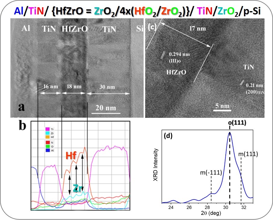
The active ferroelectric film of the NVM with TiN/Si substrate was obtained by depositing 3 types of structures based on HfO2: i) structures based on HfO2 doped with metallic Zr (HZOa– 3 versions S-01, S-02, S-03); ii) multi-layered structures with 4 or 6 pairs of HfO2/ZrO2 layers that are very thin (nanometric size) (HZOm – 7 versions S-04 – S-10); iii) multi-layered structures with 6 pairs of HfO2:Ge/HfO2 layers that are very thin (nanometric sizes) (HGOm – 2 versions S-11, S-12).
Characterization of samples was performed by XRD, XRR and HRTEM for finding the morphology and crystalline structure. The crystallization of HfO2/ZrO2 multilayer with dominant XRD component corresponding to O/T ferroelectric phase of mixed oxide of (Hf,Zr)O2 (HRTEM) is achieved in the RTA annealed HZOm film. The crystallites are extended along the whole multilayer thickness.
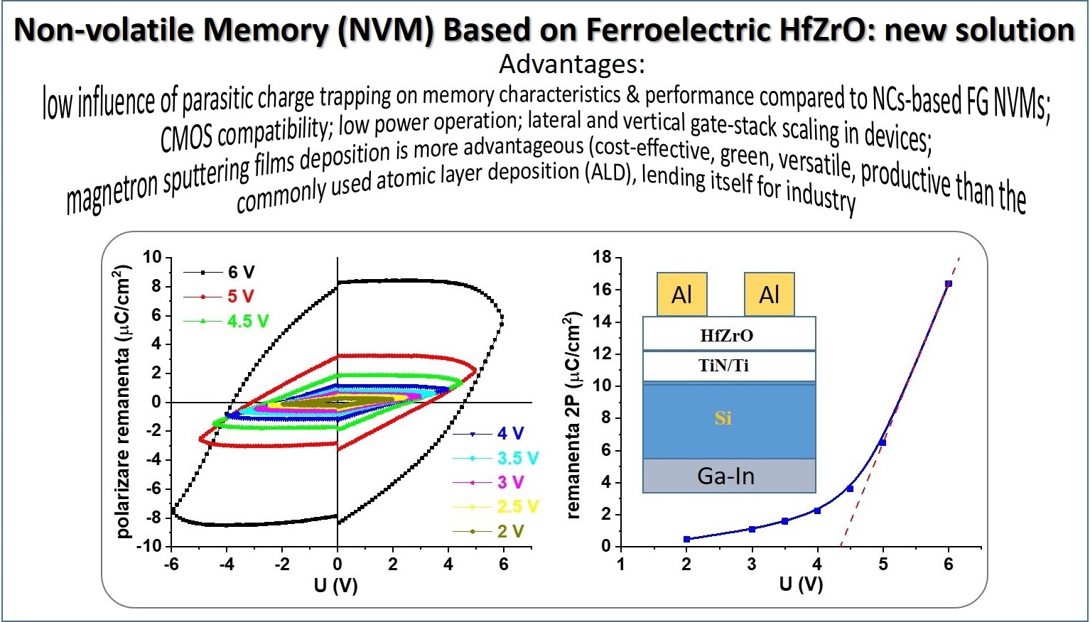
We fabricated and electrically characterized capacitor structures with Al and/or Al/TiN electrodes. The HZOm structure ZrO2 (2.2 nm)/ 4x{HfO2 (2.5 nm)/ ZrO2 (2.2 nm)}/ TiN that showed the highest remanent polarization in agreement with crystalline structure and morphology results was selected as Demonstrator. The demonstrator was functionally tested according to TRL 3, having the following memory parameters regarding remanent polarization: remanent hysteresis window of 4 V per element (1.1 MV coercive field); remanent polarization 2P (zero potential) of 16 µC/cm2.
The project web page https://infim.ro/en/project/non-volatile-memory-based-onferroelectric-hfo2-ferohafomemo/ was updated.
The proposed objectives and activities were fully achieved.
Stage 3/2022
Project FEROHAFOMEMO aims to fabricate a nonvolatile memory (NVM) based on ferroelectric HfO2, with memory window of 1.5 – 2 V and functional testing (memory characteristics) of the MNV demonstrator according to TRL 3 (proof of concept).
Stage 3/2022 has the main objective of fabricating the MNV demonstrator and its functional testing according to TRL 3 following the investigation of different test samples and selection of the best solution.
This objective was accomplished by carrying out the activities proposed for Stage 3 in Work Plan: ● Investigating memory properties (test samples) – IInd part; ● Analysis of results; selection of the best solution (test samples); ● Fabrication of NVM demonstrator – IInd part; ● Functional testing of the demonstrator according to TRL 3; ● Updating and finalizing project web page; ● Dissemination: conference paper, patent application.
In Stage 3/2022 we continued the investigation of structures based on HfO2 doped with Zr and Ge for ferroelectric NVM memories, aiming the obtaining of multi-layered structures on Si substrates covered with TiN. Characterization of samples was performed by XRD, XRR and HRTEM for finding the morphology and crystalline structure. TiN deposition was made by reactive magnetron sputtering from Ti target in Ar+N2 atmosphere or from TiN target. The active film of the ferroelectric NVM with TiN/Si substrate was obtained by depositing 3 types of structures based on HfO2: i) structures based on HfO2 doped with metallic Zr (HZOa); ii) multi-layered structures with 4 or 6 pairs of repeated HfO2/ZrO2 layers that are very thin (nanometric size) (HZOm); iii) multi-layered structures with 6 pairs of HfO2:Ge/HfO2 layers that are very thin (nanometric sizes) (HGOm). HZOm films showed remarkable properties, with dominant crystalline component corresponding to orthorhombic/tetragonal structure that produces the ferroelectric properties, while the monoclinic component contribution is weak or undetectable. The TiN layer shows columnar crystallization even from the deposition and influences the crystallization of HZOm film (HRTEM). The as-deposited HZOm film is amorphous with beginnings of crystallization induced by the columnar crystallization of TiN substrate. In the RTA annealed HZOm film, the crystallization of HfO2/ZrO2 multilayer is achieved as if a mix of Hf and Zr. It results a mixed oxide of (Hf,Zr)O2 in which the crystallites are extended along the whole multilayer thickness, resulting a mixture of orthorhombic and monoclinic phases.
For electrical measurements (I – V, P – V) regarding the performance of NVM structures, we fabricated matrices of identical nominal capacitors by using HZOm and HGOm multilayers on TiN/p-Si substrates by depositing structured Al electrodes or/and Al/TiN on the samples surface. The capacitor ferroelectric memory is formed between the top Al electrode and the TiN layer accessed through the p-Si substrate and bottom electrode from the back of Si wafer. Measurements in coplanar geometry were performed by contacting the Al electrodes from the pair of capacitors in series by the metallic TiN. The structure ZrO2 (2.2 nm)/ 4x{HfO2 (2.5 nm)/ ZrO2 (2.2 nm)}/ TiN that showed the highest remanent polarization was selected as Demonstrator and functionally tested according to TRL 3. The memory parameters of the demonstrator regarding remanent polarization are: remanent hysteresis window of 4 V per element (1.1 MV coercive field); remanent polarization 2P (zero potential) of 16 µC/cm2.
In addition to the technological achievements, we add 1 Patent Application, 1 paper published in journal with impact factor, 3 papers at international conferences. The project web page https://infim.ro/en/project/non-volatile-memory-based-onferroelectric-hfo2-ferohafomemo/ was updated. The obtained results comply with those provided in Work Plan of Stage 3.
In conclusion, the objectives and activities proposed for Stage 3/2022 were fully achieved.
Stage 2/2021
Project FEROHAFOMEMO aims to fabricate a nonvolatile memory (NVM) based on ferroelectric HfO2, with memory window of 1.5 – 2 V and good retention. This NVM device will be fabricated as demonstrator at TRL 3.
Stage 2/2021 has the main objective of investigating the morphology and structure of test NVM samples together with their characterization from point of view of NVM properties. The properties and parameters obtained from the crystalline structure and morphology characterization of structures are used for adjusting the technological parameters for achieving the project targets. In other words, electrical measurements were performed on the optimized test samples (as above described) for investigating memory properties.
This objective was accomplished by carrying out the activities proposed for Stage 2 in Work Plan: ● Magnetron sputtering (MS) deposition of test samples – IInd part; ● RTA for for obtaining of HfO2 or HfZrO ferroelectric films – IInd part; ● Configuring test samples; ● Contacts deposition; post-metallization RTA; ● Morphology and structure: testing – characterization; ● Metallic contacts – testing; ● Investigating memory properties – Ist part; ● Results analysis; selection; ● Fabrication of demonstrator – Ist part; ● Functional testing of demonstrator; ● Web page updating; ● Dissemination: ISI papers and conferences.
The capacitor–like test structures realized in this stage were deposited by magnetron sputtering followed by rapid thermal annealing – RTA at temperatures between 600 and 700 °C for the formation of HfO2 with orthorhombic/tetragonal (O/T) crystalline structure, phase that is responsible for ferroelectric properties. These test samples are the following:
- Sa: HfO2/Hf-HfO2/HfO2/p-Si (similar with the ones from Stage 1) structures of different kinds obtained by varying the thickness of intermediate Hf-HfO2 layer (50:50 composition). We labelled HfO2 5nm/Hf-HfO2 10nm/HfO2 5nm/Si-p structure as Sa10 (5/10/5), and similarly Sa15 (5/15/5) and Sa20 (5/20/5) structures.
- Sb: HfO2/Zr-HfO2/HfO2/p-Si, labelled Sb20 (5/20/5), with intermediate Zr-HfO2 layer (50:50).
- Sc: ZrO2/Zr-HfO2/ZrO2/p-Si, labelled Sc20 (5/20/5).
- Sd: ZrO2/Zr-HfO2/HfO2/p-Si, labelled Sd20 (5/20/5).
- Se: ZrO2/Zr-ZrO2/ZrO2/p-Si, labelled Se20 (5/20/5).
Complex investigations of structure and morphology properties (by Grazing Incidence XRD – GI-XRD and HRTEM) were performed for understanding and controlling the formation of O/T phase responsible for ferroelectric properties. By correlation, investigations of ferroelectric properties were carried out. GI-XRD (in good agreement with HRTEM) reveals the maxima corresponding to O/T phase of HfO2 and ZrO2 for the structures with 20 nm thick intermediate layer (e.g. Sa20, Sb20, Se20), the O/T fraction in respect to monoclinic M being reflected in parameter RO/T = 1 – RM that is dependent on the structure (Sa – Se). Additionally, the O/T fraction is maximum for Sb20 structures (for 2θ = 26.5o – 33o range in GI-XRD curves). It should be mentioned that structure Se20 has a very high RO/T fraction and very good ferroelectric memory properties.
The detailed study of structures morphology correlated with crystalline phase shows that the thin samples with intermediate layer of 10 nm thickness (Sa10 for example) are uniformly crystallized, showing only M structure with deformation, meaning that O/T phase was not observed. In the thick samples such as Sa20, there are two crystallization regions / regions with crystalline coherence, one that extends from the free surface of samples to the depth, and the other that concomitantly starts from the sample bottom, but extends in the opposite direction. We showed that the crystallization process is dependent on the oxygen concentration, and the speed of crystallization front depends on the speed of oxygen diffusion. These two crystallization regions have O/T crystalline structure, namely the top region presents O/T phase mainly at the interface with and inside the intermediate layer (crystallization front advances inside this layer), while the bottom region is practically O/T.
Structures Sa20 (600-4 and 650-4 RTA), Sd20 (600-8 and 650-4), and Se20 (600-8, 650-4 and 650-8) present P – V hysteresis loops up to 20 Hz frequencies, with memory window ΔV values corresponding to project target. Structure Se 650-4 has the best ferroelectric properties, for which ΔV = 4.46 V.
Project web page https://infim.ro/en/project/non-volatile-memory-based-on-ferroelectric-hfo2-ferohafomemo/ was updated.
The obtained results are in good agreement with those provided in Work Plan of Stage 2.
In conclusion, the objectives and activities proposed for Stage 2/2021 were fully achieved.
Stage 1/2020
The project FEROHAFOMEMO aims to fabricate a nonvolatile memory (NVM) based on ferroelectric HfO2 as demonstrator up to TRL, having targeted parameters of 1.5 – 2 V memory window and good retention.
Stage 1/2020 has the main objective of obtaining technological parameters correlated with the morphology for fabrication of test samples. This objective has been achieved by the following activities: ● magnetron sputtering (MS) deposition of test samples – 1st part; ● rapid thermal annealing (RTA) for obtaining of HfO2 or HfZrO ferroelectric films – 1st part; ● Test of morphology and structure; ● project web page setup and continuous updating.
In this stage, 2 types of capacitor–like test structures of HfO2/Hf-HfO2/HfO2/Si-p were realized. They differ to each other by the size of Hf-HfO2 intermediary layer. We define by Sa (5/10/5) the structure of HfO2 5nm/Hf-HfO2 10nm /HfO2 5nm /Si-p and analogously Sb (5/20/5). The structures were deposited by MS followed by RTA at 600 oC for 4 and 8 min respectively, in N2 flux of 100 sccm for the formation of ferroelectric HfO2 (orthorhombic phase).
The morphology and structure of these samples were investigated (XRD, HRTEM and modelling) together with the ferroelectric properties.
Both structures present in XRD curves maxima corresponding to orthorhombic/tetragonal phase, Sb 600-4 structure having the maximum corresponding to orthorhombic phase more intense than Sb 600-8. HRTEM images show that Sb 600-8 sample has a morphology with 2 different zones having completely different crystalline coherence. So, the film surface zone is of monoclinic HfO2, while orthorhombic/tetragonal HfO2 phases are located at the bottom of film. The crystalline coherence covers the whole thickness of bottom zone (11-12 nm). HfO2 crystallites with different structures are separated to each other by damaged zones. So, the monoclinic and orthorhombic crystallites respectively, present a continuity of the crystalline planes alignment with similar lattice fringes. This demonstrates that the transition from a crystalline structure to the other one takes place during the crystal growth (crystallization process).
The characteristics of electrical polarization – voltage, P – V, taken on both samples Sa and Sb that were RTA annealed at 600 oC for 4 and 8 min show that these structures have ferroelectric properties. P – V characteristics present hysteresis loops up to 30-40 Hz frequencies.
We have to remark that Sa 600-8 and Sb 600-4 have the best ferroelectric properties.
The project web page: https://infim.ro/en/project/non-volatile-memory-based-on-ferroelectric-hfo2-ferohafomemo/.
The obtained results are in good agreement with those provided in Realization Plan of Stage 1.
In conclusion, the objectives and activities proposed for Stage 1/2020 were fully achieved.
Papers published in journals with impact factor
- „Memory properties of Zr doped ZrO2 MOS-like capacitor”, C. Palade, A. Slav, I. Stavarache, V.A. Maraloiu, C. Negrila, M.L. Ciurea, Coatings 12, 1369 (2022)
- „SiGeSn quantum dots in HfO2 for floating gate memory capacitors”, C. Palade, A. Slav, O. Cojocaru, V.S. Teodorescu, T. Stoica, M.L. Ciurea, A.M. Lepadatu, Coatings 12, 348 (2022)
- „A nanoscale continuous transition from the monoclinic to ferroelectric orthorhombic phase inside HfO2 nanocrystals stabilized by HfO2 capping and self-controlled Ge doping”, C. Palade, A.M. Lepadatu, A. Slav, O. Cojocaru, A. Iuga, V.A. Maraloiu, A. Moldovan, M. Dinescu, V.S. Teodorescu, T. Stoica, M.L. Ciurea, Journal of Materials Chemistry C 9, 12353 (2021)
Papers indexed in international databases (Scopus, Web of Science)
- „Memory properties of GeZrO2 based trilayer structure”, C. Palade, A. Slav, M.L. Ciurea, IEEE International Semiconductor Conference CAS 2021 Proceedings, ISBN: 978-0-7381-2665-4, pages 253-256, IEEE 2021
- „In-situ magnetron sputtering co-deposition of Ge nanoparticles in Si3N4 films for near infrared detection”, I. Stavarache, C. Palade, P. Prepelita, V.S. Teodorescu, M.L. Ciurea, IEEE International Semiconductor Conference CAS 2021 Proceedings, ISBN: 978-0-7381-2665-4, pages 261-264, IEEE 2021
Patent application
- OSIM patent application no. A/00433 (July 21st 2022) „Procedeu de obtinere a unei structuri de memorie nevolatila pe baza de ZrHfO2 feroelectric” („Fabrication method for obtaining a non-volatile memory structure based on ferroelectric ZrHfO2”), C. Palade, I. Stavarache, A. Slav, A.M. Lepadatu, T. Stoica, M.L. Ciurea
Conference presentations
- „Ferroelectric HfO2/Ge-HfO2/HfO2 3-layer nonvolatile memory based on orthorhombic Ge doped HfO2 assisted by stress”, M.L. Ciurea, C. Palade, A.M. Lepadatu, A. Slav, O. Cojocaru, A. Iuga, V.A. Maraloiu, A. Moldovan, M. Dinescu, V.S. Teodorescu, T. Stoica, IEEE International Semiconductor Conference (CAS) 45th edition CAS 2022, Poiana Brasov, October 12 -14, 2022, https://www.imt.ro/cas/invited_speakers.php#; invited presentation
- „Ferroelectric HfO2 phase formation by Ge-doping in HfO2/Ge-HfO2/HfO2 3-layer structures assisted by stress field”, C. Palade, A.M. Lepadatu, A. Slav, O. Cojocaru, A. Iuga, V.A. Maraloiu, A. Moldovan, M. Dinescu, V.S. Teodorescu, T. Stoica, M.L. Ciurea, 20th International Balkan Workshop on Applied Physics and Materials Science – IBWAP 2022, Constanta, July 12-15, 2022, http://ibwap.ro/; invited presentation
- „Ferroelectric Ge-doped HfO2 by HfO2 capping”, Palade, A.M. Lepadatu, A. Slav, O. Cojocaru, A. Iuga, V.A. Maraloiu, A. Moldovan, M. Dinescu, V.S. Teodorescu, T. Stoica, M.L. Ciurea, 2022 Spring Meeting of the European Materials Research Society - E-MRS, May 30 - June 3, 2022, https://www.european-mrs.com/synthesis-processing-and-characterization-nanoscale-multi-functional-oxide-films-viii-and-6th-e-mrs; oral presentation
- „Rapid thermal annealing temperature effects on charge storage behavior of SiGeSn quantum dots embedded in the high-k CMOS-compatible HfO2 in floating gate non-volatile memories”, C. Palade, A. Slav, O. Cojocaru, V.S. Teodorescu, T. Stoica, M.L. Ciurea, A.M. Lepadatu, 20th International Balkan Workshop on Applied Physics and Materials Science – IBWAP 2022, Constanta, July 12-15, 2022, http://ibwap.ro/; oral presentation
- „Ferroelectric orthorhombic HfO2 phase in 3-layer memory structures of control HfO2 /floating gate of Ge nanoparticles in HfO2 /tunnel HfO2 on Si wafers”, C. Palade, A.M. Lepadatu, A. Slav, O. Cojocaru, A. Iuga, V.A. Maraloiu, A. Moldovan, M. Dinescu, V.S. Teodorescu, T. Stoica, M.L. Ciurea, Materials Challenges for Memory - MCFM 2021, April 11-13, 2021, https://horizons.aip.org/materials-challenges/; poster
- „Memory properties of GeZrO2 based trilayer structure”, Palade, A. Slav, M.L. Ciurea, IEEE International Semiconductor Conference - CAS 2021, October 6-8, 2021, https://www.imt.ro/cas/programme_2021.php; poster
Dr. Magdalena Lidia Ciurea - ciurea@infim.ro
PROJECTS / NATIONAL PROJECTS