This project proposes developing a synaptic structure based on HfOx/GexSn1-x with conductance modulated by the ferroelectric field-effect. By improving the ferroelectric characteristics of HfO2 using a high-mobility channel material (epi/poly GeSn), we obtain a synaptic neuron-like structure that simulates a three-terminal memristor for neuromorphic computing. The HfOx/GexSn1-x structure is obtained by reactive/non-reactive magnetron sputtering followed by Rapid Thermal Annealing in active working gas (H2/N2) to avoid the local disorder by passivating the dangling bonds and by healing the trap states. The plasticity of synaptic neuron-like structure HfOx/GexSn1-x will be modulated and enhanced by controlling the interface between HfO2 FeCAP and GeSn high-mobility channel.
CS III Dr. Adrian Slav (https://www.brainmap.ro/adrian-slav) - Project Coordinator
CS II Dr. Ionel Stavarache (https://www.brainmap.ro/ionel-stavarache) - Experienced Researcher
CS II Dr. Ana-Maria Lepadatu (https://www.brainmap.ro/ana-maria-lepadatu) - Experienced Researcher
CS II Dr. Valentin Adrian Maraloiu (https://www.brainmap.ro/valentin-adrian-maraloiu) - Experienced Researcher
CS III Dr. George Adrian Lungu (https://www.brainmap.ro/george-adrian-lungu) - Experienced Researcher
CS Dr. Catalin Palade (https://www.brainmap.ro/catalin-palade) - Postdoc
ACS Dr. Ioana Maria Avram Dascalescu (https://www.brainmap.ro/ioana-maria-avram-dascalescu) - Postdoc
ACS Ovidiu Cojocaru (https://www.brainmap.ro/ovidiu-cojocaru) - PhD Student (PhD Adviser Dr. M.L. Ciurea)
Stage I/2022
In this stage, preliminary technological parameters were obtained for the deposition by magnetron sputtering (MS) of HfO2 and GexSn1-x films to create HfO2/GexSn1-x neuronal-type synaptic structures. GeSn films were obtained by co-deposition in DC mode from separate Ge and Sn targets. GeSn nanocrystals (NC) and the crystallization of HfO2 layers are formed by RTA thermal treatments in a hydrogen atmosphere. After the thermal treatments of the GeSn layers, crystallization is initiated from 350 oC with a slight formation of β - Sn, and at 450 oC we obtain a clear separation of the two constituent phases, Ge, respectively β - Sn. In the case of the HfO2/GeSn structure, the amorphous state is maintained up to 250 oC; above this temperature, the formation of GeSn NCs begins, which is very clearly evident at 450 oC, without the formation of the β-Sn phase. Above 450 oC, the crystallization of the HfO2 layer begins, which at 550 oC shows a mixture of monoclinic and orthorhombic phases together with GeSn NCs. The absence of β-Sn phase formation up to temperatures above 500 oC in the case of HfO2/GeSn structures compared to GeSn films can be explained by the appearance of stress at the interface of GeSn with HfO2 during deposition. This stress can be due to the flow of atoms reaching the support and their energy (translated experimentally by the deposition rate and the power applied to the magnetron) and/or by the implantation of atomic hydrogen in the structure. Through XRR measurements, the density of 8.5 g/cm3 (ρHfO2= 9.68 g/cm3-bulk) and the roughness of 0.7 nm for the HfO2 layer and the density of 5.42g/cm3 (ρGe= 5.32 g/cm3-bulk, ρSn= 7.3 g/cm3-bulk) and the roughness of 1.2 nm for the GeSn layers. From the analysis of the Raman spectra obtained at various values of the incident laser power, the concentration of Sn in the GeSn NC was obtained between 6.3% and 8.2% Sn concentration in GeSn NCs. For the nanostructures treated by RTA at 250 oC, 550 oC and without thermal treatment, a residual polarization of ~1 μC/cm2 was obtained, and the shape of the hysteresis curve shows the capacitive character combined with ohmic conduction caused by the formation of β - Sn.
Stage II/2023
In this stage, by carrying out all the activities stipulated in the Project Realization Plan, the following has been obtained:
- deposition of synaptic-type neuronal structures starting from depositions by MS (magnetron sputtering) of HfO2/Ge/Sn/HfO2/c-Si type, in which a GeSn layer has been crystallized through Metal Induced Crystallization (MIC) method, with conduction qualities superior to HfO2/GeSnHfO2/[GeSn/HfO2]×4/GeSn/p-Si(100) multilayer structures;
- experimental process parameters for the deposition by MS of synaptic structures and post-deposition RTA treatment conditions for achieving crystallization;
- evaluation of the electric response of the neuronal synapse-type structures to pulses applied at a certain frequency to the gate contact (modulation of the current through the conduction channel formed by GeSn by voltage pulses applied on the gate);
Stage III/2024
During this stage, the following results have been obtained:
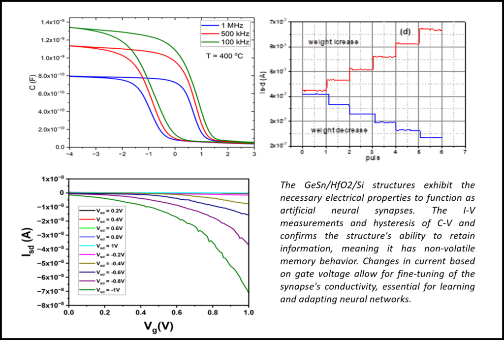
- The ferroelectric character of the HfO2 gate layer in the HfOx/GexSn1-x neural synaptic structures was investigated through remanent polarization measurements on samples treated with RTA at 250 and 450 °C. A remanent polarization of ~0.5 μC/cm² and ~0.3 μC/cm² at V = 0V was obtained for samples thermally treated at 250 °C and 550 °C, respectively, with a pulse of ± 1V/5s;
- To highlight the field effect, source-drain current versus gate voltage measurements were performed. The source-drain current was measured while maintaining different constant voltage values during the application of gate voltage;
- Measurements were conducted to test the plasticity of the synaptic structure by applying a pulsed writing signal and measuring the source-drain current. Practically, a pulsed voltage in the range of 0-1 V was applied, with pulses of various durations. The measurements highlighted the change in the synaptic structure's weight through the current jump, concurrent with a change in the curve's slope after a certain number of pulses. Additionally, these weight changes depend not only on the voltage value and the number of pulses but also on the pulse application time. Practically, the state of the synapse depends on the strength and persistence of the writing signal.
- The training capability of the HfO2/GexSn1-x/HfO2 synaptic device is evaluated by measuring the channel conductance as a function of the number of pulses, with specific modulation of width and amplitude. The gate voltage VG regulates the carrier concentration of the GeSn semiconductor channel through partial polarization switching, thus controlling the IS-D current, making it possible to access and program multiple states of the artificial neural synapse.
Articles published in ISI-quoted journals:
- C. Palade, A. Slav, I. Stavarache, V.A. Maraloiu, C. Negrila, M.L. Ciurea, "Memory properties of Zr doped ZrO2 MOS-like capacitor", Coatings 2022, 12(9), 1369; https://doi.org/10.3390/coatings12091369
- I. Dascalescu, A. Slav, C. Palade, G.A. Lungu, V.S Teodorescu, M. Braic, M.L. Ciurea , T. Stoica, "Influence of in-situ hydrogenation on photoelectrical properties of amorphous and nanocrystalline GeSn deposited by magnetron sputtering", ACS Applied Materials & Interfaces, manuscript ID am-2024-09877r
International Conference presentations
- Oral presentation: "Enhanced Photoconductivity Of Hydrogeneted GeSn Thin Films ",
I. Dascalescu, A. Slav, C. Palade, G. A. Lungu, Ana M. Lepadatu, O. Cojocaru, V. S. Teodorescu,
M. L. Ciurea, M. Braic, T. Stoica, 21st International Balkan Workshop on Applied Physics and Materials Science, 11–14 July 2023, Constanta, Romania. - Oral presentation: "SWIR extended photoconductivity in a hydrogeneted GeSn films",
I. Dascalescu, A. Slav, C. Palade, G. A. Lungu, A.M. Lepadatu, V. S. Teodorescu, M. Braic, M.L. Ciurea, T. Stoica , International Semiconductor Conference, 11–13 October 2023, Sinaia, Romania. - Oral presentation (on-line): "GexSn1-x thin film with high spectral response in SWIR range deposited by magnetron sputtering", A. Slav, C. Palade, I. Stavarache, G. A. Lungu, M. Braic, S. Iftimie, V.S. Teodorescu, M.L. Ciurea, T. Stoica, 14th International Conference on Physics of Advanced Materials (ICPAM-14), Dubrovnik, Croatia
Project Contact Person:
Project Director: Dr. Adrian Slav
National Institute of Materials Physics, Atomistilor 405A., 077125 Magurele - Bucharest, ROMANIA
Tel:+40--(0)21-2418-151
Email: slav.infim.ro
PROJECTS / NATIONAL PROJECTS