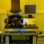
Photolithography Mask Aligner EVG 620 NT with Nanoimprint Litography (EV Group)
FACILITIES / NANOMATERIALE

The equipment for optical litography allows for selectively masking and exposing of certain areas of the sample surface, using a “mask” or a set of masks. Masks are realized in advance by laser etching a thin metalic layer deposited onto a special glass slide.
Masking is necessary for the operations of selective etching or “lift-off”. “Photoresist” is the generic name of a specially formulated chemical, usually liquid which is spread across the sample surface by high speed spinning. After drying, selective exposure to ultraviolet (UV) light through a mask, developing and thermal treatment, the photoresist gets special properties to protecting the sample surface against the chemicals employed for selective etching of the sample surface. As one can see in the processing record below, processing a device requires up to 20-30 cleanroom steps and an operation, as the photolithography, can be employed several times, depending on the complexity. Selectivity and spatial resolution of optical litography is limited to 1-2 microns. The nanolithography facility of SEM (Scanning Electron Microscope) employs an electron beam with a very small spot and allows for masking areas and features less than a micron in size, directly on to the sample and fully computer controlled, without the need for additional set of masks or intermediary operations of processing the photoresist.
Technical Specifications of EVG620NT (EV Group GmbH):
Mask Aligner
- Exposure modes: hard-, soft- and vacuum contact
- Proximity separation distance 0-300 μm adjustable via software
- Wafer thickness 0.1 – 10 mm
- Semi automatic loading with mechanical prealignment 5 Ms-Windows® -based process software for recipes, diagnostic and operation
- Unlimited storage of recipes
- Remote diagnostics
- 500 W Hg UV lamp
- Alignment stage with precision micrometers
- Automatic wedge compensation
- WEC contact force 0.5 – 40 N adjustable
- Mask holder for 4” x 4” masks with loading frame
- Vacuum Contact wafer chuck 3” , 2” and pieces
Tooling for Soft UV-Nanoimprinting and Micro Contact Printing
- Tool set for soft UV-NIL and μ-CP
- PDMS stamp mounted on glass backplane (5” square)
- Top chuck for min 1” and max. 100 mm stamp diameter
- Bottom chuck for 100 mm wafer
- Contact-free wedge compansation with spacers
- Adjustable contact force for vacuum printing process
- Dedicated Software for NanoImprint Lithography (NIL)
Copyright © 2025 National Institute of Materials Physics. All Rights Reserved