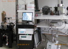
The experimental system developed in the last years serves to measure magneto-transport, electrical, electro-optical, parametric, high Z, DC, RF, photoelectric, ferroelectric and microwave properties, as well as the electrical characteristics of the electrically active defects generated during the growth, implantation, processing or irradiation of the materials and test devices.
Two Janis cryostats, each with 4 optical windows, dedicated to measure one in the temperature range from 20K to 475 K and the other between 77K and 800K. Both cryostats are connected to turbo-molecular vacuum pumps.
Gratting Monochromator Oriel, wavelengths 200-6000 nm, with chopper for modulating the frequency up to 1 kHz for photoelectric signal.
Keithley electrometers (2) with incorporated sources for voltages up to 1000 V. Currents as low as 10 fA can be measured with these electrometers.
Agilent and Hioki RC bridges for capacitance measurements with frequencies up to 5 MHz.
Probe-station CPX-VF equipped with 4 probe arms, each with 3-axis adjustments and ±5° theta planarization, and a 25 kOe vertical field superconducting magnet. The temperature range for the probe station is from 4.2 K to 400 K and the measuring frequencies from DC to 67 GHz. The system can operate with external equipment, such as oscilloscopes, RC bridges, electrometers, etc.
TF Analyzer 2000 for measuring properties of non-linear dielectrics such as: Hysteresis, Fatigue, Retention, Static hysteresis, Imprint, Leakage current. The system can operate with external equipment, such as oscilloscopes, temperature units, probing stations, high voltage amplifiers, etc.

The last two characterization facilities were purchased in 2009 and were integrally supported from the infrastructure POS-CCE Project of NIMP „Euro-Regional Centre for Advanced Materials, for Surfaces and Interfaces”, Project-No. 141/2009, acronym CEUREMAVSU.

HERA-DLTS HE-1030 and TSC Systems for detection and characterization of electrically active defects in materials and structures. The electrically active defects generated during the growth, implantation, processing or irradiation are those that has a direct impact on the electrical properties of the materials, multilayer structures and complex devices. Their detection and characterization is essential for improving the growth and processing technologies. The system is sensitive to defects generated in concentration as low as 108 cm-3 and it is an unique facility in our country.