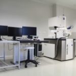
Electron lithography equipment – High resolution installation
FACILITIES / NANOFABRICATION-OF-MATERIALS

Equipment for high resolution electron printing that will be used to realize various types of structures and electrical contacts on nano-objects supergrid periodic applications in photonics and other metallization with complex geometries required for the development of advanced materials structures, for different applications.
TECHNICAL SPECIFICATIONS
- High resolution electron lithography equipment will combine high-resolution scanning electron microscope system for high resolution imaging and writing user-defined structures, design and control system, for achieving actual lithographic structures. Using electrons, the imaging system is high resolution based on an electron emission source type with better resolution than, or equal to 0.8 nm;
- MERLIN Compact Base Unit with column GEMINI I, oil-free pumping system, microscope room with 3 ports for 3 EDS, automatic pendulum to prevent vibration, platform with 5 eucentric motorized axis and dual joystick control. The SE detector in the microscope room, DoF-module, scope chamber, carousel with support for 9 samples and 24“ TFT monitor;
- XDS10 pumping system;
- High-resolution configuration for the vacuum system with a Gemini I column and a 20nA sample current;
- System integrated in the Gemini lense column I with 2 detection modes: the detection of secondary electrons and backscatter electron detection (parallel detection of SE and BSE electrons is not possible);
- High accuracy Everhard Thornley secondary electron detector (replaces standard detectors). It allows a very high scan speed compared to standard detectors, but with the same ratio signal/noise;
- Plasma Cleaner with integrated software and Smart SEM microscope software;
- An EDX port adapter for DN40-KF (for attaching the Plasma Cleaner);
- The imaging allows detection of secondary electrons and electron backscattering;
- The system allows automatic correction of electron beam drift;
- Lithography process control system provides ultra-high resolution that allows writing individual user-defined fields; it contains a beam blanker system (shutter beam) lithography experiments;
- The system assures the control of high-resolution lithography processes, which allows writing to both individual user-defined fields and on a beam blanker system that contains (a shutter beam) lithography experiments;
- Multiple fields for coverage of large areas (stitching);
- The system has a sample-holding table with a powerful positioning system with a resolution of better than 2 nm.
Copyright © 2026 National Institute of Materials Physics. All Rights Reserved