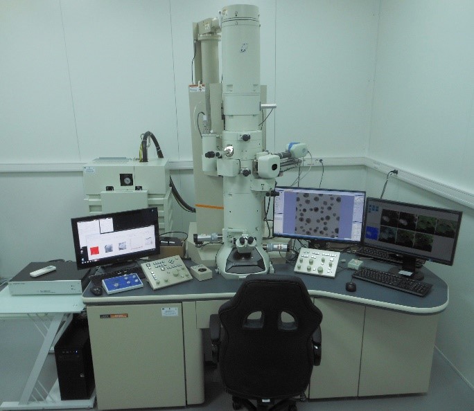
A multifunctional tool, designed for the research and characterization of advanced materials, used for the following types of studies: conventional TEM, HRTEM, STEM, electron tomography, precession electron diffraction (PED), in-situ TEM at high or cryogenic temperatures, energy dispersive X-ray spectroscopy, elemental chemical mapping.
- Configuration: LaB6 gun, STEM unit, JEOL JED-2300T Dry SDD EDS unit, emSIS Tengra bottom-mounted CCD camera, NanoMEGAS ASTAR PED unit, tomography kit for TEM/STEM including electron tomography holder and software platform for automated TEM/STEM image acquisition at predefined tilting angles, 3D image reconstruction and visualization;
- Technical specifications: Acceleration voltage 80-200 kV; TEM point resolution 0.23 nm; STEM resolution 1 nm; EDS spectral resolution 125 eV;
- Working modes: CTEM/HRTEM, SAED, nano-ED, CBED, STEM (BF, ADF), EDS, e-tomography, PED