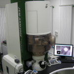
JEM-ARM200F Atomic Resolution Transmission Electron Microscope
FACILITIES / ELECTRON-MICROSCOPY

Aberration corrected analytical instrument designed for atomic resolution characterization of advanced materials by imaging (HRTEM, STEM) and spectroscopic (EELS, EDS) methods.
- Configuration: Schottky Field Emission Gun (FEG), CEOS spherical aberration corrector for STEM mode, STEM Unit, Gatan Quantum SE EELS and Image Filter, JEOL JED-2300T EDS unit, Gatan Orius 200D CCD (wide angle port), Gatan Ultrascan 1000XP (bottom mounted CCD), Gatan Ultrascan 1000FT (GIF CCD)
- Technical specifications: Acceleration voltages 120 and 200 kV; TEM point resolution 0.19 nm; STEM resolution 0.08 nm; EELS spectral resolution 0.7 eV; EDS spectral resolution 133 eV;
- Working modes: HRTEM, STEM (BF, ADF, HAADF), CTEM, SAED, nano-ED, CBED, EDS, EELS, EFTEM, EELS-SI
Copyright © 2026 National Institute of Materials Physics. All Rights Reserved