Photoemission and low energy electron microscopy (LEEM, PEEM)
FACILITIES / STIINTA-SUPRAFETEI

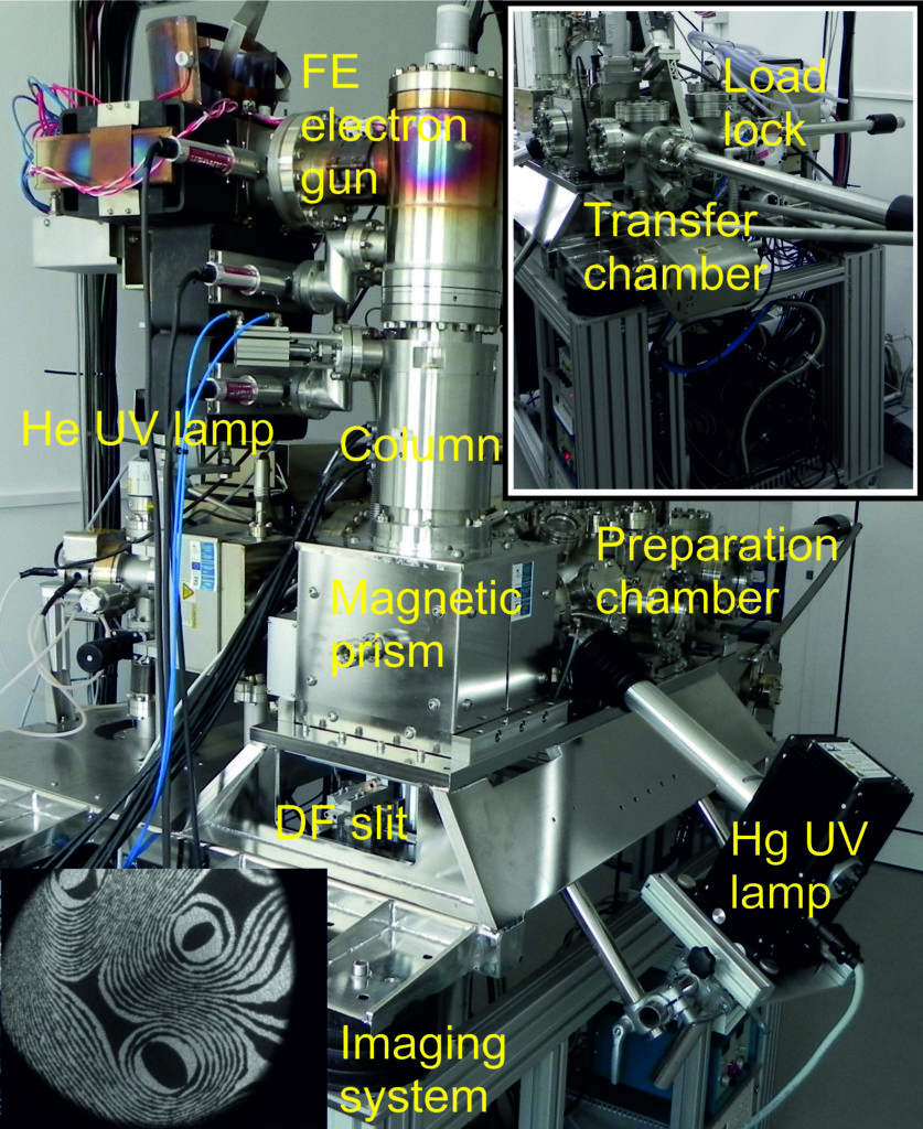
An installation for low energy and photoemission electron microscopy: LEEM – PEEM, micro LEED, micro ARUPS (Specs, Fig. 4). The installation is able to perform simultaneous imaging (i. e. without scanning) of surfaces by using low energy electrons or photoelectrons produced by UV radiation. In the LEEM mode, the lateral resolution is about 5 nm, and in the PEEM mode about 50 nm. The advantages of using this installation are (i) the possibility to record immediate imaging, to realize movies, to fllow-up in real time surface modifications; (ii) the fact that one uses low energy electrons makes this method suitable for delicate surfaces, which otherwise would be damaged by high energy electrons such as the ones used in scanning electron microscopy (SEM); (iii) one may obtain structural or electronic structure (densities of states, dispersion laws) information on nanometer scale.

Copyright © 2026 National Institute of Materials Physics. All Rights Reserved